


TMS320TCI648x DSP
Multichannel Buffered Serial Port (McBSP)
User's Guide
Literature Number: SPRU803C
December 2005–Revised May 2010

2
SPRU803C–December 2005–Revised May 2010
Copyright © 2005–2010, Texas Instruments Incorporated

Preface ....................................................................................................................................... 8
1 Features ........................................................................................................................... 10
2 McBSP Interface ................................................................................................................ 11
3 McBSP Overview ............................................................................................................... 13
3.1 Resetting the Serial Port: RRST, XRST, GRST, and RESET ................................................... 13
3.2 Determining Ready Status ............................................................................................ 14
3.3 CPU Interrupts: RINT, XINT .......................................................................................... 14
3.4 Frame and Clock Configuration ...................................................................................... 15
4 Clocks, Frames, and Data ................................................................................................... 16
4.1 Frame and Clock Operation .......................................................................................... 17
4.2 Sample Rate Generator Clocking and Framing .................................................................... 18
4.3 Data Clock Generation ................................................................................................ 19
4.4 Frame Sync Generation ............................................................................................... 23
4.5 Data and Frames ...................................................................................................... 25
4.6 Clocking and Framing Examples .................................................................................... 29
5 McBSP Standard Operation ................................................................................................ 34
5.1 Receive Operation ..................................................................................................... 34
5.2 Transmit Operation .................................................................................................... 35
5.3 Maximum Frame Frequency .......................................................................................... 35
5.4 Frame Synchronization Ignore ....................................................................................... 36
5.5 Serial Port Exception Conditions .................................................................................... 39
6 m-Law/A-Law Companding Hardware Operation .................................................................... 45
6.1 Companding Internal Data ............................................................................................ 46
6.2 Bit Ordering ............................................................................................................. 46
7 McBSP Initialization Procedure ........................................................................................... 47
7.1 General Initialization Procedure ...................................................................................... 47
7.2 Special Case: External Device is the Transmit Frame Master ................................................... 49
8 Multichannel Selection Operation ........................................................................................ 51
8.1 Enabling Multichannel Selection ..................................................................................... 51
8.2 Enabling and Masking of Channels in Normal Multichannel Selection Mode .................................. 51
8.3 Changing Element Selection ......................................................................................... 54
8.4 End-of-Subframe Interrupt ............................................................................................ 54
8.5 Enhanced Multichannel Selection Mode ............................................................................ 55
8.6 DX Enabler: DXENA ................................................................................................... 56
9 SPI Protocol: CLKSTP ........................................................................................................ 57
9.1 McBSP Operation as the SPI Master ............................................................................... 59
9.2 McBSP Operation as the SPI Slave ................................................................................. 59
9.3 McBSP Initialization for SPI Mode ................................................................................... 60
10 McBSP Pins as General-Purpose I/O .................................................................................... 61
11 McBSP Registers ............................................................................................................... 62
11.1 Data Receive Register (DRR) ........................................................................................ 63
11.2 Data Transmit Register (DXR) ....................................................................................... 64
3
SPRU803C–December 2005–Revised May 2010 Table of Contents
Copyright © 2005–2010, Texas Instruments Incorporated

www.ti.com
11.3 Serial Port Control Register (SPCR) ................................................................................ 65
11.4 Receive Control Register (RCR) ..................................................................................... 68
11.5 Transmit Control Register (XCR) .................................................................................... 75
11.6 Sample Rate Generator Register (SRGR) ......................................................................... 82
11.7 Multichannel Control Register (MCR) ............................................................................... 83
11.8 Receive Channel Enable Register (RCER) ........................................................................ 85
11.9 Transmit Channel Enable Registers (XCER) ...................................................................... 86
11.10 Enhanced Receive Channel Enable Registers (RCERE0-3) .................................................... 87
11.11 Enhanced Transmit Channel Enable Registers (XCERE0-3) .................................................... 90
11.12 Pin Control Register (PCR) .......................................................................................... 96
Appendix A Revision History ...................................................................................................... 98
4
Contents SPRU803C–December 2005–Revised May 2010
Copyright © 2005–2010, Texas Instruments Incorporated

www.ti.com
List of Figures
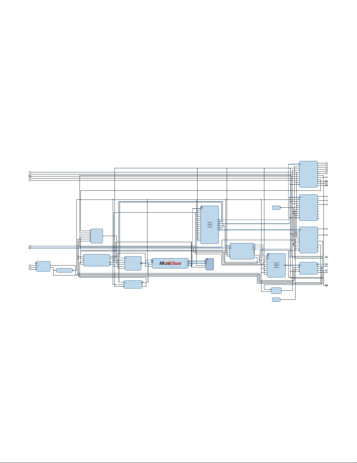
1 McBSP Block Diagram.................................................................................................... 11
2 Frame and Clock Operation.............................................................................................. 15
3 Clock and Frame Generation ............................................................................................ 16
4 Receive Data Clocking.................................................................................................... 17
5 Transmit Data Clocking................................................................................................... 17
6 Sample Rate Generator .................................................................................................. 18
7 CLKG Synchronization and FSG Generation When GSYNC = 1 and CLKGDV = 1 ............................. 20
8 CLKG Synchronization and FSG Generation When GSYNC = 1 and CLKGDV = 3 ............................. 21
9 Programmable Frame Period and Width ............................................................................... 23
10 Dual-Phase Frame Example ............................................................................................. 25
11 Single-Phase Frame and Four 8-Bit Elements ........................................................................ 27
12 Single-Phase Frame of One 32-Bit Element .......................................................................... 27
13 Data Delay.................................................................................................................. 28
14 Bit Data Delay Used to Discard Framing Bit........................................................................... 28
15 AC97 Dual-Phase Frame Format ....................................................................................... 30
16 AC97 Bit Timing Near Frame Synchronization ........................................................................ 30
17 McBSP to ST-BUS Block Diagram...................................................................................... 31
18 Double-Rate ST-BUS Clock Example .................................................................................. 31
19 Single-Rate ST-BUS Clock Example ................................................................................... 32
20 Double-Rate Clock Example ............................................................................................. 33
21 McBSP Standard Operation.............................................................................................. 34
22 Receive Operation......................................................................................................... 34
23 Transmit Operation........................................................................................................ 35
24 Maximum Frame Frequency for Transmit and Receive .............................................................. 35
25 Unexpected Frame Synchronization With (R/X) FIG = 0 ............................................................ 36
26 Unexpected Frame Synchronization With (R/X)FIG = 1 ............................................................. 37
27 Maximum Frame Frequency Operation with 8-Bit Data .............................................................. 38
28 Data Packing at Maximum Frame Frequency With (R/X)FIG = 1................................................... 39
29 Serial Port Overrun........................................................................................................ 40
30 Serial Port Receive Overrun Avoided................................................................................... 40
31 Decision Tree Response to Receive Frame Synchronization Pulse................................................ 41
32 Unexpected Receive Synchronization Pulse .......................................................................... 41
33 Transmit With Data Overwrite ........................................................................................... 42
34 Transmit Empty ............................................................................................................ 43
35 Transmit Empty Avoided ................................................................................................. 43
36 Decision Tree Response to Transmit Frame Synchronization Pulse............................................... 44
37 Unexpected Transmit Frame Synchronization Pulse ................................................................. 44
38 Companding Flow ......................................................................................................... 45
39 Companding Data Formats .............................................................................................. 45
40 Transmit Data Companding Format in DXR ........................................................................... 45
41 Companding of Internal Data ............................................................................................ 46
42 Element Enabling by Subframes in Partitions A and B............................................................... 52
43 XMCM = 00b FOR XMCM Operation................................................................................... 53
44 XMCM - 01b, XPABLK = 00b, XCER = 1010b for XMCM Operation............................................... 53
45 XMCM = 10b, XPABLK = 00b, XCER = 1010b for XMCM Operation.............................................. 53
46 XMCM = 11b, RPABLK = 00b, XPABLK = X, RCER = 1010b, XCER = 1000b for XMCM Operation......... 54
47 DX Timing for Multichannel Operation.................................................................................. 56
5
SPRU803C–December 2005–Revised May 2010 List of Figures
Copyright © 2005–2010, Texas Instruments Incorporated


