l298中文资料 步进电机驱动

L298
Jenuary 2000
DUAL FULL-BRIDGE DRIVER
Multiwatt15
ORDERING NUMBERS : L298N (Multiwatt Vert.)
L298HN (Multiwatt Horiz.)
L298P (PowerSO20)
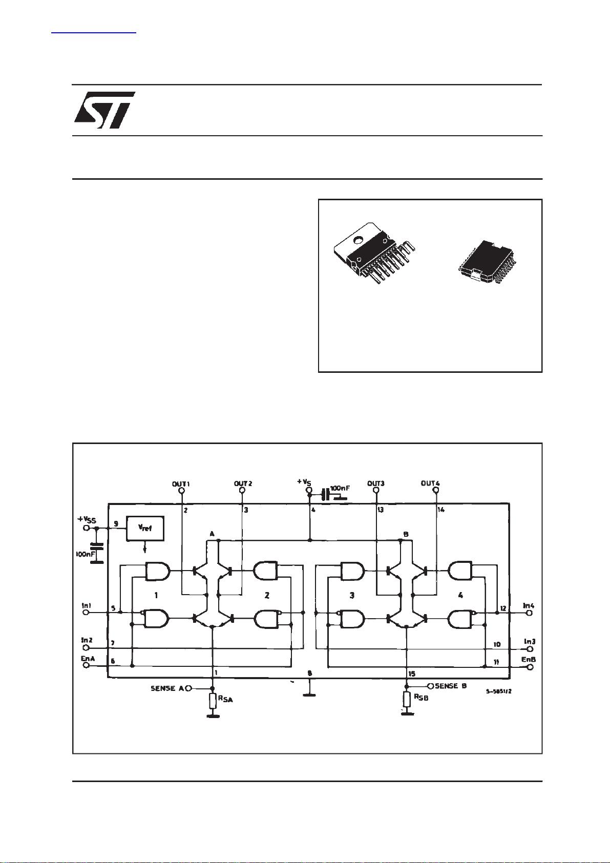
BLOCK DIAGRAM
.OPERATING SUPPLYVOLTAGEUP TO 46 V
.TOTAL DC CURRENT UP TO 4 A
.
LOW SATURATION VOLTAGE
.OVERTEMPERATURE PROTECTION
.
LOGICAL ”0” INPUT VOLTAGE UP TO 1.5 V
(HIGH NOISE IMMUNITY)
DESCRIPTION
The L298 is an integratedmonolithic circuit in a 15-
lead Multiwatt and PowerSO20 packages. It is a
high voltage,high current dual full-bridge driver de-
signedto acceptstandardTTL logiclevelsanddrive
inductive loads such as relays, solenoids, DC and
steppingmotors. Two enableinputsare providedto
enableor disablethe deviceindependentlyofthein-
put signals. The emitters of the lower transistors of
each bridge are connected togetherand the corre-
spondingexternalterminal can be used for the con-
nectionofanexternalsensingresistor.Anadditional
supplyinput is provided so that the logic works at a
lower voltage.
PowerSO20
1/13
查询L298供应商


剩余12页未读,继续阅读
资源评论

 www4611960412011-11-09英文的,是真的。
w359602111
- 粉丝: 0
- 资源: 2


最新资源
- Python闭包:深入理解与应用场景解析.zip
- Win64OpenSSL-3-3-0.exe
- 课高分程设计-基于C++实现的民航飞行与地图简易管理系统-南京航空航天大学
- 航天器遥测数据故障检测系统python源码+文档说明+数据库(课程设计)
- 北京航空航天大学操作系统课设+ppt+实验报告
- 基于Vue+Echarts实现风力发电机中传感器的数据展示监控可视化系统+源代码+文档说明(高分课程设计)
- 基于单片机的风力发电机转速控制源码
- 基于C++实现的风力发电气动平衡监测系统+源代码+测量数据(高分课程设计)
- 毕业设计- 基于STM32F103C8T6 单片机,物联网技术的太阳能发电装置+源代码+文档说明+架构图+界面截图
- 基于 LSTM(长短期记忆)(即改进的循环神经网络)预测风力发电厂中风力涡轮机产生的功率+源代码+文档说明
资源上传下载、课程学习等过程中有任何疑问或建议,欢迎提出宝贵意见哦~我们会及时处理!
点击此处反馈


