没有合适的资源?快使用搜索试试~ 我知道了~
DA14582 BLE Data Sheet
5星 · 超过95%的资源 需积分: 9 68 下载量 193 浏览量
2015-11-03
13:46:06
上传
评论
收藏 1.45MB PDF 举报
温馨提示
试读
177页
Dialog DA14582 BLE with voice support data sheet
资源推荐
资源详情
资源评论
© 2015 Dialog Semiconductor 1 www.dialog-semiconductor.com
DA14582 Low Power Bluetooth Smart SoC with Audio Codec
DATASHEET -
General description
The DA14582 integrated circuit has a fully integrated
radio transceiver, baseband processor for Bluetooth
®
Smart with Audio Codec.
The DA14582 is optimized for remote control units
(RCU) requiring support for voice commands and
motion/gesture recognition. Its integrated analog wide
band audio codec provides native support for analog
microphones thereby reducing the total number of
components of the system while its optimized package
enables designs using single-layer FR1 PCBs further-
more contributing to the reduction of the cost of the
system.
The DA14582 supports a flexible memory architecture
for storing Bluetooth profiles and custom application
code, which can be updated over the air (OTA). The
qualified Bluetooth Smart protocol stack is stored in a
dedicated ROM. All software runs on the ARM® Cor-
tex®-M0 processor via a simple scheduler.
The Bluetooth Smart firmware includes the L2CAP ser-
vice layer protocols, Security Manager (SM), Attribute
Protocol (ATT), the Generic Attribute Profile (GATT)
and the Generic Access Profile (GAP). All profiles pub-
lished by the Bluetooth SIG as well as custom profiles
are supported.
The transceiver interfaces directly to the antenna and
is fully compliant with the Bluetooth 4.1 standard.
The DA14582 has dedicated hardware for the Link
Layer implementation of Bluetooth
®
Smart and inter-
face controllers for enhanced connectivity capabilities.
Features
Complies with Bluetooth V4.1, ETSI EN 300 328 and
EN 300 440 Class 2 (Europe), FCC CFR47 Part 15
(US) and ARIB STD-T66 (Japan)
Processing power
16 MHz 32 bit ARM Cortex-M0 with SWD I/F
Dedicated Link Layer Processor
AES-128 bit encryption Processor
Memories
32 kB One-Time-Programmable (OTP) memory
42 kB System SRAM
84 kB ROM
8 kB Retention SRAM
Power management
Integrated Buck DC-DC converter
P0, P1, P2 and P3 ports with 3.3 V tolerance
Easy decoupling of only 4 supply pins
Supports coin (typ. 3.0 V) and alkaline (typ. 1.5 V)
battery cells
10-bit ADC for battery voltage measurement
Digital controlled oscillators
16 MHz crystal (±20 ppm max) and RC oscillator
32 kHz crystal (±50 ppm, ±500 ppm max) and
RCX oscillator
General purpose, Capture and Sleep timers
Digital interfaces
29 General purpose I/Os
2 UARTs with hardware flow control up to 1 MBd
SPI+™ interface
I2C bus at 100 kHz, 400 kHz
3-axis capable Quadrature Decoder
Analog interfaces
4-channel 10-bit ADC
14 bits wide band Codec with microphone and
28 loudspeaker analog front-end
Radio transceiver
Fully integrated 2.4 GHz CMOS transceiver
Single wire antenna: no RF matching or RX/TX
switching required
Supply current at VBAT3V:
TX: 3.4 mA, RX: 3.7 mA (with ideal DC-DC)
0 dBm transmit output power
-20 dBm output power in “Near Field Mode”
-93 dBm receiver sensitivity
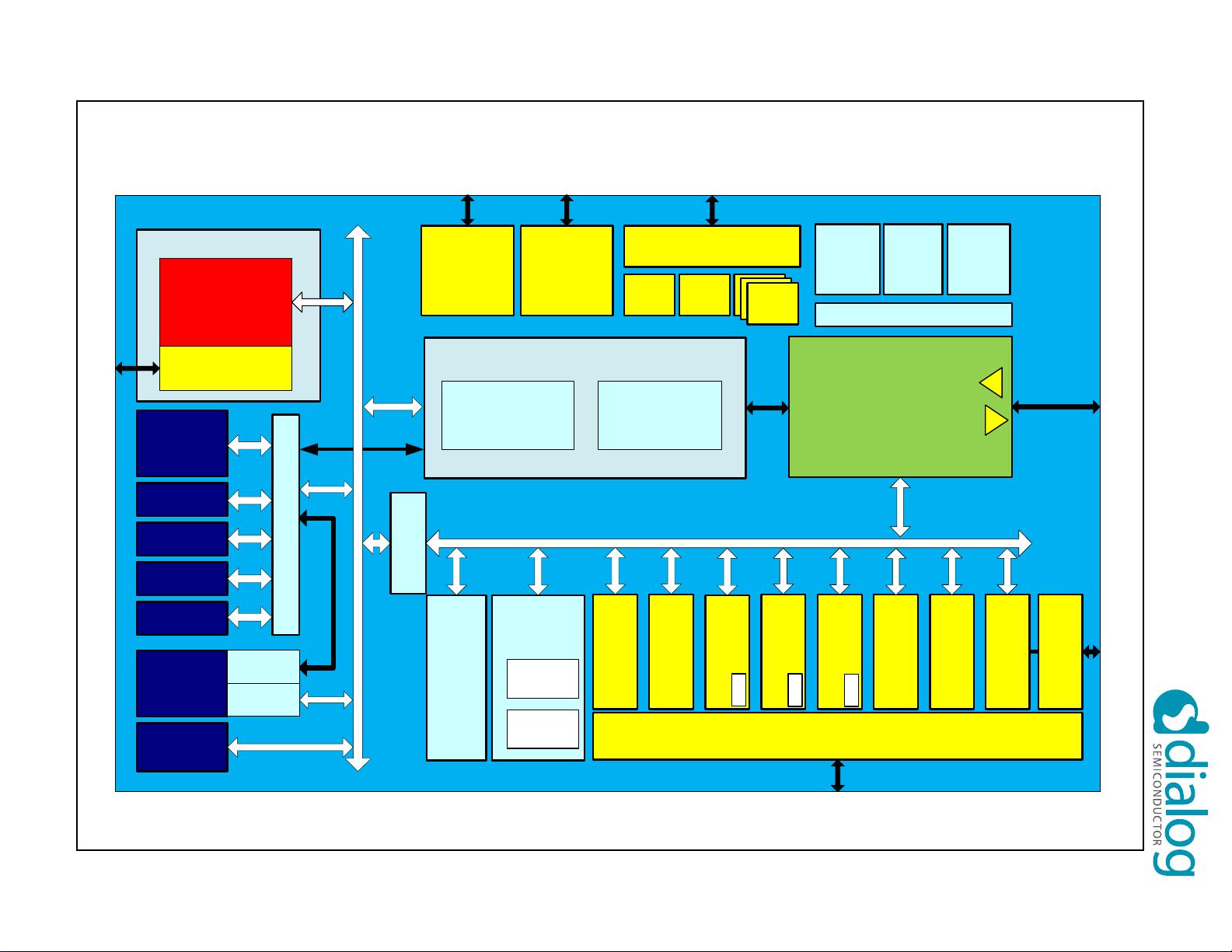
________________________________________________________________________________________________
System diagram
MARCH 11, 2015 V2.0
DA14582
Low Power Bluetooth Smart SoC with Audio Codec
PRELIMINARY
DA14582 Low Power Bluetooth Smart SoC with Audio Codec
© 2015 Dialog Semiconductor 1 Preliminary - March 11, 2015 v2.0
1. Block diagram. . . . . . . . . . . . . . . . . . . . . . . . . . . . . . 2
2. Pinout . . . . . . . . . . . . . . . . . . . . . . . . . . . . . . . . . . . . 3
3. System overview . . . . . . . . . . . . . . . . . . . . . . . . . . . 7
3.1 ARM CORTEXM0 CPU . . . . . . . . . . . . . . . . . . 7
3.2 BLUETOOTH SMART. . . . . . . . . . . . . . . . . . . . 7
3.2.1 BLE Core . . . . . . . . . . . . . . . . . . . . . . . . . 7
3.2.2 Radio Transceiver . . . . . . . . . . . . . . . . . . 8
3.2.3 SmartSnippets
3.3 MEMORIES . . . . . . . . . . . . . . . . . . . . . . . . . . . . 9
3.4 FUNCTIONAL MODES . . . . . . . . . . . . . . . . . . . 9
3.5 POWER MODES. . . . . . . . . . . . . . . . . . . . . . . 10
3.6 INTERFACES . . . . . . . . . . . . . . . . . . . . . . . . . 10
3.6.1 UARTs . . . . . . . . . . . . . . . . . . . . . . . . . . 10
3.6.2 SPI+ . . . . . . . . . . . . . . . . . . . . . . . . . . . . 10
3.6.3 I2C interface . . . . . . . . . . . . . . . . . . . . . 10
3.6.4 General purpose ADC . . . . . . . . . . . . . . 11
3.6.5 Quadrature decoder. . . . . . . . . . . . . . . . 11
3.6.6 Keyboard controller . . . . . . . . . . . . . . . . 11
3.6.7 Input/output ports. . . . . . . . . . . . . . . . . . 11
3.7 TIMERS . . . . . . . . . . . . . . . . . . . . . . . . . . . . . . 11
3.7.1 General purpose timers . . . . . . . . . . . . . 11
3.7.2 Wake-Up timer . . . . . . . . . . . . . . . . . . . . 12
3.7.3 Watchdog timer . . . . . . . . . . . . . . . . . . . 12
3.8 CLOCK/RESET . . . . . . . . . . . . . . . . . . . . . . . . 12
3.8.1 Clocks . . . . . . . . . . . . . . . . . . . . . . . . . . 12
3.8.2 Reset . . . . . . . . . . . . . . . . . . . . . . . . . . . 12
3.9 POWER MANAGEMENT . . . . . . . . . . . . . . . . 13
3.10 AUDIO CODEC WITH ANALOG FRONTEND15
4. Specifications . . . . . . . . . . . . . . . . . . . . . . . . . . . . . 16
5. Codec specifications . . . . . . . . . . . . . . . . . . . . . . . 27
5.1 CODEC ELECTRICAL CHARACTERISTICS . 28
5.2 ANALOG FRONTEND SPECIFICATIONS . . . 30
5.3 CODEC SPECIFICATIONS . . . . . . . . . . . . . . 34
5.4 CODEC TIMING CHARACTERISTICS. . . . . . 38
6. Registers . . . . . . . . . . . . . . . . . . . . . . . . . . . . . . . . . 39
6.1 CODEC REGISTER FILE . . . . . . . . . . . . . . . 164
7. Package information . . . . . . . . . . . . . . . . . . . . . . 174
7.1 MOISTURE SENSITIVITY LEVEL (MSL) . . . 174
7.2 SOLDERING INFORMATION . . . . . . . . . . . . 174
7.3 PACKAGE OUTLINES . . . . . . . . . . . . . . . . . 175
DA14582 Low Power Bluetooth Smart SoC with Audio Codec
© 2015 Dialog Semiconductor 2 Preliminary - March 11, 2015 v2.0
1. Block diagram
Figure 1 DA14582 block diagram
24 April 2012
ARM Cortex M0
SWD (JTAG)
CORE
POReset
BLE Core
LINK LAYER
HARDWARE
AES-128
Radio
Transceiver
APB bridge
POWER/CLOCK
Management (PMU)
DCDC
(BUCK/BOOST)
GPIO MULTIPLEXING
XTAL
16 MHz
XTAL
32.768 kHz
RC
32 kHz
SW TIMER
GP ADC
ROM
84 KB
System/
Exchange
RAM
42 KB
Ret. RAM
2 KB
RC
16 MHz
Memory Controller
OTP
32 KB
DMA
OTPC
QUAD
DECODER
LDO
SYS
LDO
RET
LDO
SYS
LDO
SYS
LDO
RF
WAKE UP
TIMER
Ret. RAM2
3 KB
Ret. RAM3
2 KB
Ret. RAM4
1 KB
KEYBOARD
CTRL
UART
FIFO
UART2
FIFO
I2C
FIFO
RCX
Timer 0
1xPWM
Timer 2
3xPWM
SPI
CODEC
DA14582 Low Power Bluetooth Smart SoC with Audio Codec
© 2015 Dialog Semiconductor 3 Preliminary - March 11, 2015 v2.0
2. Pinout
Figure 2 QFN56 pin assignment
13-Jan-2015
RFIOp
P0_3
P3_0
P0_4/SPI_DI
P0_5/16MCLK
P0_6
VDDIO
GPIO3
P2_1/SPI_EN
GPIO2
XTAL32Kp
P2_2
VBAT_RF
VREFp
MICp
XTAL32Km
XTAL16Mm
XTAL16Mp
P1_3
P1_2
SW_CLK
SWDIO
P1_1
PVBAT1V
SWITCH
P1_0
VPP
P2_8
P2_7
RFIOm
P2_6
P2_5
55
P3_7
P2_9
54
53
52
51
50
49
48
47
46
P0_2
RSTn
VDCDC_RF
56
P2_0
P3_3
VBAT3V
P3_5
P3_6
44
43
P2_4
P2_3
VDCDC
RST
VDD
LSRn
P0_0
P0_1
45
GND
VBUF
VREFm
MICp
LSRp
P0_7
Pin 58: GND plane
Pin 57: GND plane
DA14582
(top view)
1
2
4
3
5
6
7
9
8
10
11
12
14
13
42
41
40
39
38
37
36
35
34
33
32
31
30
29
15
16
17
18
19
20
21
22
23
24
25
26
27
28
Table 1: Ordering information
Part number Package Size (mm) Shipment form Pack quantity
DA14582-01KA1 QFN56 8 x 8 Tray 50 (Samples)
DA14582-01KA2 QFN56 8 x 8 Reel 3000 (Production
DA14582 Low Power Bluetooth Smart SoC with Audio Codec
© 2015 Dialog Semiconductor 4 Preliminary - March 11, 2015 v2.0
Table 2: Pin Description
PIN NAME TYPE
Drive
(mA)
Reset
state
(Note )
DESCRIPTION
General Purpose I/Os
P0_0
P0_1
P0_2
P0_3/
P0_4/SPI_DI
P0_5/16MCLK
P0_6
P0_7
DIO
DIO
DIO
DIO
DIO
DIO
DIO
DIO
4.8 I-PD
I-PD
I-PD
I-PD
I-PD
I-PD
I-PD
I-PD
INPUT/OUTPUT with selectable pull up/down resistor. Pull-
down enabled during and after reset. General purpose I/O port
bit or alternate function nodes. Contains state retention mecha-
nism during power down.
P1_0
P1_1
P1_2
P1_3
P1_4/SWCLK
P1_5/SW_DIO
DIO
DIO
DIO
DIO
DIO
DIO
4.8 I-PD
I-PD
I-PD
I-PD
I-PD
I-PU
INPUT/OUTPUT with selectable pull up/down resistor. Pull-
down enabled during and after reset. General purpose I/O port
bit or alternate function nodes. Contains state retention mecha-
nism during power down.
This signal is the JTAG clock by default
This signal is the JTAG data I/O by default
P2_0
P2_1/SPI_EN
P2_2
P2_3
P2_4
P2_5
P2_6
P2_7
P2_8
P2_9
DIO
DIO
DIO
DIO
DIO
DIO
DIO
DIO
DIO
DIO
4.8 I-PD
I-PD
I-PD
I-PD
I-PD
I-PD
I-PD
I-PD
I-PD
I-PD
INPUT/OUTPUT with selectable pull up/down resistor. Pull-
down enabled during and after reset. General purpose I/O port
bit or alternate function nodes. Contains state retention mecha-
nism during power down.
P3_0
P3_1 (Table 3)
P3_2 (Table 3)
P3_3
P3_5
P3_6
P3_7
DIO
DIO
DIO
DIO
DIO
DIO
DIO
4.8 I-PD
I-PD
I-PD
I-PD
I-PD
I-PD
I-PD
INPUT/OUTPUT with selectable pull up/down resistor. Pull-
down enabled during and after reset. General purpose I/O port
bit or alternate function nodes. Contains state retention mecha-
nism during power down.
Debug interface
SW_DIO/P1_5 DIO 4.8 I-PU INPUT/OUTPUT. JTAG Data input/output. Bidirectional data and
control communication. Can also be used as a GPIO
SW_CLK/P1_4 DIO 4.8 I-PD INPUT JTAG clock signal. Can also be used as a GPIO
Clocks
XTAL16Mp AI INPUT. Crystal input for the 16 MHz XTAL
XTAL16Mm AO OUTPUT. Crystal output for the 16 MHz XTAL
XTAL32kp AI INPUT. Crystal input for the 32.768 kHz XTAL
XTAL32km AO OUTPUT. Crystal output for the 32.768 kHz XTAL
剩余176页未读,继续阅读
资源评论
- issacf2016-12-13能用到的资源~
- fromlens2017-08-18很好的文档
u010132897
- 粉丝: 1
- 资源: 1
上传资源 快速赚钱
- 我的内容管理 展开
- 我的资源 快来上传第一个资源
- 我的收益 登录查看自己的收益
- 我的积分 登录查看自己的积分
- 我的C币 登录后查看C币余额
- 我的收藏
- 我的下载
- 下载帮助
安全验证
文档复制为VIP权益,开通VIP直接复制
信息提交成功