没有合适的资源?快使用搜索试试~ 我知道了~
cmos sensor introduction
需积分: 17 11 下载量 162 浏览量
2008-12-09
13:15:41
上传
评论 1
收藏 2.37MB PDF 举报
温馨提示
试读
15页
cmos摄像头传感器介绍 An introduction to the technology,design and performance limits,presenting recent developments and future directions.
资源推荐
资源详情
资源评论
■ 6
IEEE CIRCUITS & DEVICES MAGAZINE
■
MAY/JUNE 2005
8755-3996/05/$20.00 ©2005 IEEE
T
he market for solid-state image sensors
has been experiencing explosive growth
in recent years due to the increasing
demands of mobile imaging, digital still
and video cameras, Internet-based video con-
ferencing, surveillance, and biometrics. With
over 230 million parts shipped in 2004 and an
estimated annual growth rate of over 28% (In-
Stat/MDR), image sensors have become a sig-
nificant silicon technology driver.
Charge-coupled devices (CCDs) have tradi-
tionally been the dominant image-sensor tech-
nology. Recent advances in the design of image
sensors implemented in complementary metal-
oxide semiconductor (CMOS) technologies have
led to their adoption in several high-volume
products, such as the optical mouse, PC cam-
eras, mobile phones, and high-end digital cam-
eras, making them a viable alternative to CCDs.
Additionally, by exploiting the ability to integrate
sensing with analog and digital processing
down to the pixel level, new types of CMOS
imaging devices are being created for man-
machine interface, surveillance and monitor-
ing, machine vision, and biological testing,
among other applications.
In this article, we provide a basic introduc-
tion to CMOS image-sensor technology, design,
and performance limits and present recent
Abbas El Gamal
and Helmy Eltoukhy
©DIGITALVISION, LTD.
7 ■
IEEE CIRCUITS & DEVICES MAGAZINE
■
MAY/JUNE 2005
developments and future directions in
this area. We begin with a brief
description of a typical digital imaging
system pipeline. We also discuss
image-sensor operation and describe
the most popular CMOS image-sensor
architectures. We note the main non-
idealities that limit CMOS image sen-
sor performance, and specify several
key performance measures. One of the
most important advantages of CMOS
image sensors over CCDs is the ability
to integrate sensing with analog and
digital processing down to the pixel
level. Finally, we focus on recent devel-
opments and future research directions that are enabled by
pixel-level processing, the applications of which promise to
further improve CMOS image sensor performance and broaden
their applicability beyond current markets.
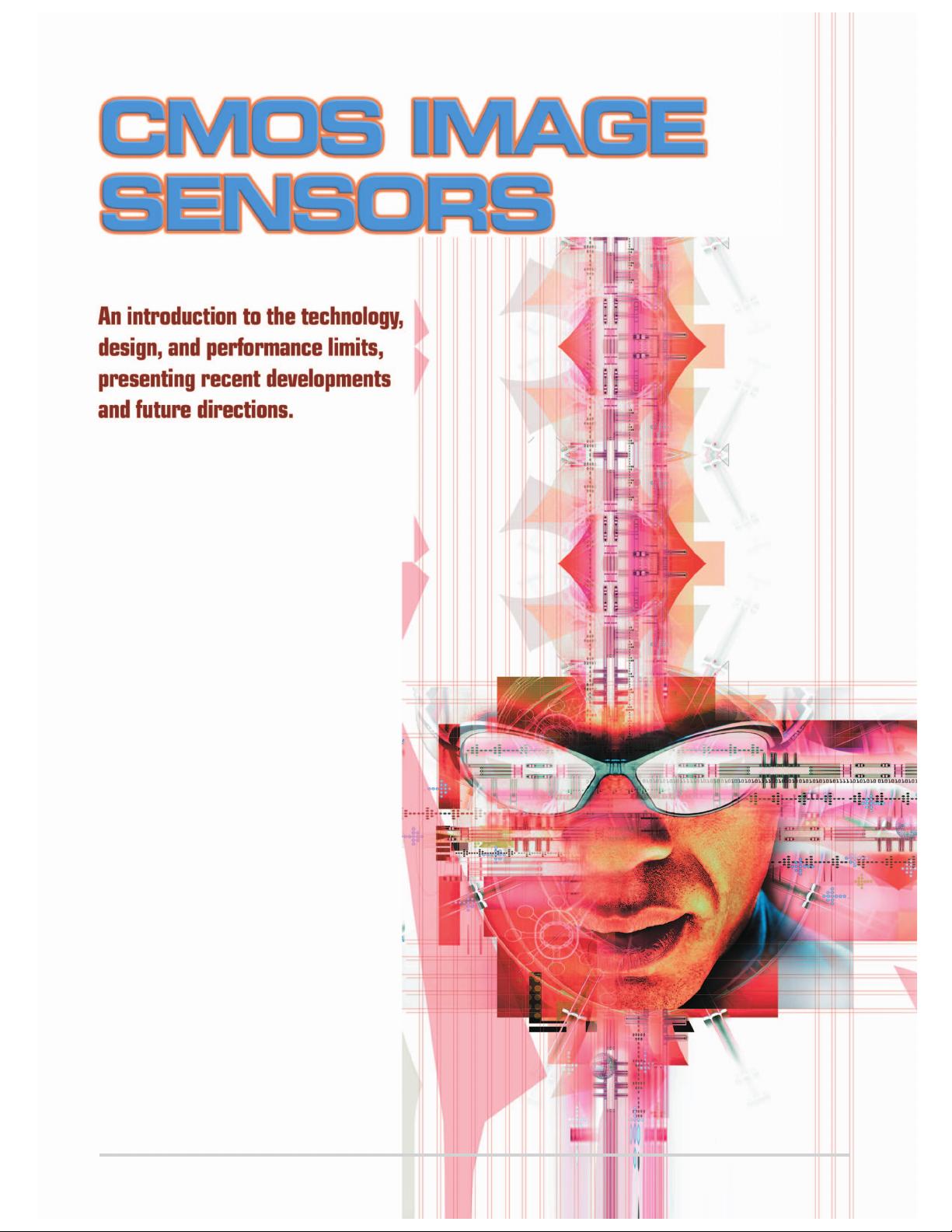
IMAGING SYSTEM PIPELINE
An image sensor is one of the main building blocks in a digital
imaging system such as a digital still or video camera. Figure
1 depicts a simplified block diagram of an imaging-system
architecture. First, the scene is focused on the image sensor
using the imaging optics. An image sensor comprising a two-
dimensional array of pixels converts the light incident at its
surface into an array of electrical signals.
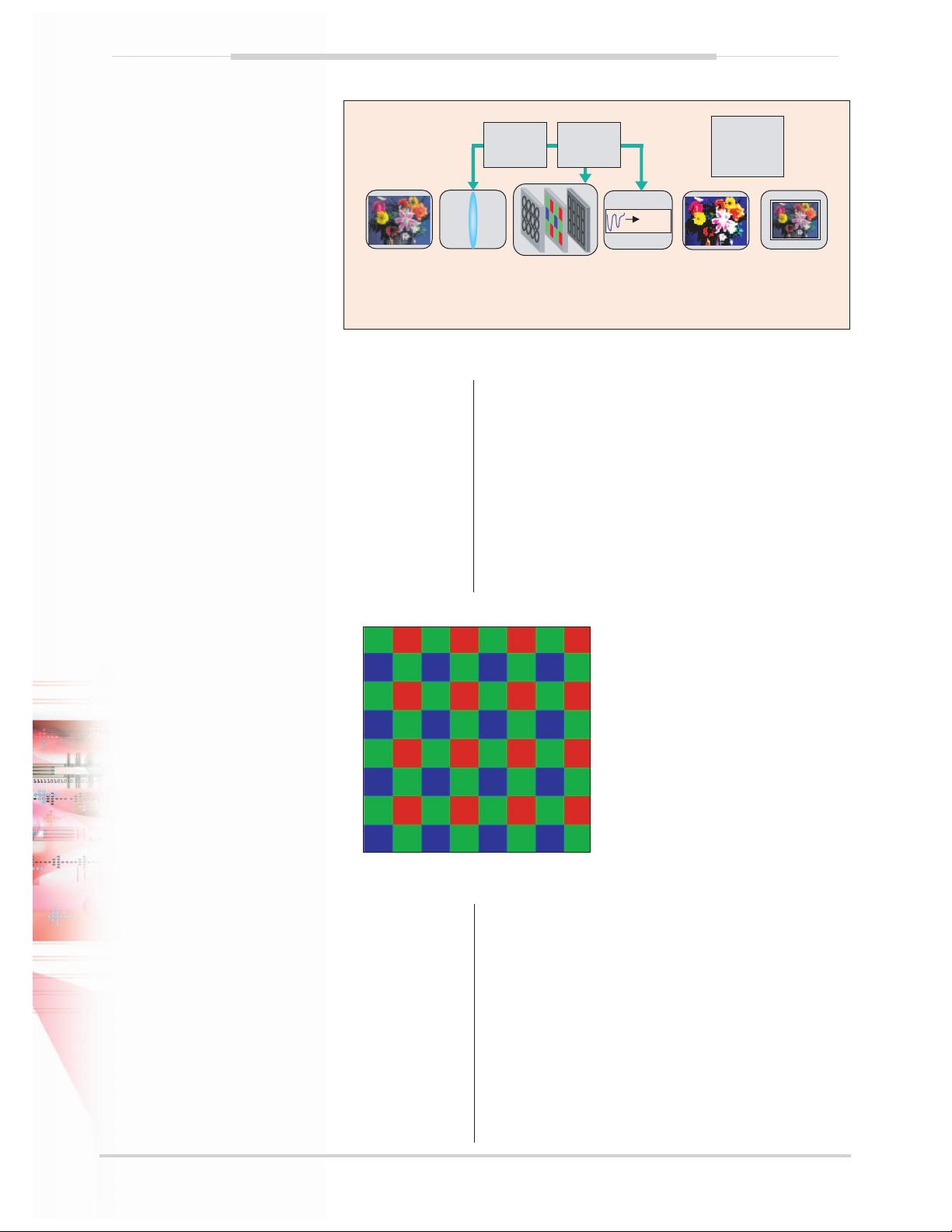
To perform color imaging, a color-filter-
array (CFA) is typically deposited in a cer-
tain pattern on top of the image sensor
pixel array (see Figure 2 for a typical red-
green-green-blue Bayer CFA). Using such
a filter, each pixel produces a signal corre-
sponding to only one of the three colors,
e.g., red, green, or blue. The analog pixel
data (i.e., the electrical signals) are read
out of the image sensor and digitized by
an analog-to-digital converter (ADC). To
produce a full color image, i.e., one with
red, green and blue color values for each
pixel, a spatial interpolation operation
known as demosaicking is used. Further
digital-signal processing is used to perform white balancing
and color correction as well as to diminish the adverse effects
of faulty pixels and imperfect optics. Finally, the image is
compressed and stored in memory. Other processing and con-
trol operations are also included for performing auto-focus,
auto-exposure, and general camera control.
Each component of an imaging system plays a role in
determining its overall performance. Simulations [1] and
experience, however, show that it is the image sensor that
often sets the ultimate performance limit. As a result, there
has been much work on improving image sensor performance
through technology and architecture enhancements as dis-
cussed in subsequent sections.
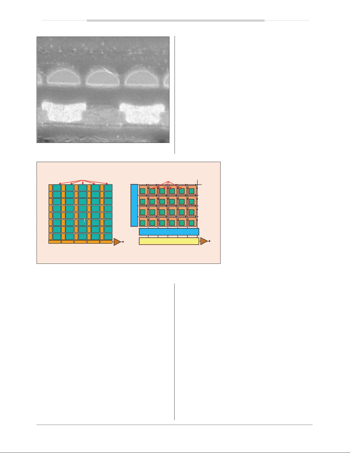
IMAGE-SENSOR ARCHITECTURES
An area image sensor consists of an array of pixels, each con-
taining a photodetector that converts incident light into pho-
tocurrent and some of the readout circuits needed to convert
the photocurrent into electric charge or voltage and to read it
off the array. The percentage of area occupied by the photode-
tector in a pixel is known as fill factor. The rest of the readout
circuits are located at the periphery of the array and are mul-
tiplexed by the pixels. Array sizes can be as large as tens of
megapixels for high-end applications, while individual pixel
sizes can be as small 2
×
2
µ
m. A microlens array is typically
deposited on top of the pixel array to increase the amount of
light incident on each photodetector.
Figure 3 is a scanning electron micro-
scope (SEM) photograph of a CMOS
image sensor showing the color filter and
microlens layers on top of the pixel array.
The earliest solid-state image sensors
were the bipolar and MOS photodiode
arrays developed by Westinghouse, IBM,
Plessy, and Fairchild in the late 1960s [2].
Invented in 1970 as an analog memory
device, CCDs quickly became the domi-
nant image sensor technology. Although
several MOS image sensors were reported
in the early 1980s, today’s CMOS image
sensors are based on work done starting
around the mid 1980s at VLSI Vision Ltd
and the Jet Propulsion Laboratory. Up until the early 1990s,
the passive pixel sensor (PPS) was the CMOS image sensor
technology of choice [3]. The feature sizes of the available
CMOS technologies were too large to accommodate more
than the single transistor and three interconnect lines in a
PPS pixel. PPS devices, however, had much lower perfor-
mance than CCDs, which limited their applicability to low-end
machine-vision applications. In the early 1990s, work began
on the modern CMOS active pixel sensor (APS), conceived
originally in 1968 [4], [5]. It was quickly realized that adding
an amplifier to each pixel significantly increases sensor speed
and improves its signal-to-noise ratio (SNR), thus overcoming
the shortcomings of PPS. CMOS technology feature sizes,
1. The imaging system pipeline.
Control and
Interface
AGC
ADC
Color
Processing
Scene Imaging
Optics
011…
Auto
Focus
Auto
Exposure
Image
Enhancement
and
Compression
Microlens Array
Color Filter Array
Image Sensor
2. The color filter array Bayer pattern.
■ 8
IEEE CIRCUITS & DEVICES MAGAZINE
■
MAY/JUNE 2005
however, were still too large to make APS commercially viable.
With the advent of deep submicron CMOS and integrated
microlens technologies, APS has made CMOS image sensors a
viable alternative to CCDs. Taking further advantage of tech-
nology scaling, the digital pixel sensor (DPS), first reported in
[6], integrates an ADC at each pixel. The massively parallel
conversion and digital readout provide very high speed read-
out, enabling new applications such as wider dynamic range
(DR) imaging, which is discussed later in this article.
Many of the differences between CCD and CMOS image
sensors arise from differences in their readout architectures.
In a CCD [see Figure 4(a)], charge is shifted out of the array
via vertical and horizontal CCDs, converted into voltage via a
simple follower amplifier, and then serially read out. In a
CMOS image sensor, charge voltage signals are read out one
row at a time in a manner similar to a random access memory
using row and column select circuits [see Figure 4(b)]. Each
readout architecture has its advantages and disadvantages.
The main advantage of the CCD readout architecture is that it
requires minimal pixel overhead, making it possible to design
image sensors with very small pixel sizes. Another important
advantage is that charge transfer is passive and therefore does
not introduce temporal noise or pixel to pixel variations due
to device mismatches, known as fixed-pattern noise (FPN).
The readout path in a CMOS image sensor, by comparison,
comprises several active devices that introduce both temporal
noise and FPN. Charge transfer readout, however, is serial
resulting in limited readout speed. It is also high power due to
the need for high-rate, high-voltage clocks to achieve near-
perfect charge transfer efficiency. By comparison, the random
access readout of CMOS image sensors provides the potential
for high-speed readout and window-of-interest operations at
low power consumption. There are several recent examples of
CMOS image sensors operating at hundreds of frames per sec-
ond with megapixel or more resolution [7]–[9]. The high-
speed readout also makes CMOS image sensors ideally suited
for implementing very high-resolution imagers with multi-
megapixel resolutions, especially for
video applications. Recent examples of
such high-resolution CMOS imagers
include the 11-megapixel sensor used
in the Canon EOS-1 camera and the 14-
megapixel sensor used in the Kodak
DCS camera.
Other differences between CCDs and
CMOS image sensors arise from differ-
ences in their fabrication technologies.
CCDs are fabricated in specialized tech-
nologies solely optimized for imaging
and charge transfer. Control over the
fabrication technology also makes it
possible to scale pixel size down with-
out significant degradation in perfor-
mance. The disadvantage of using such
specialized technologies, however, is
the inability to integrate other camera
functions on the same chip with the sensor. CMOS image sen-
sors, on the other hand, are fabricated in mostly standard
technologies and thus can be readily integrated with other
analog and digital processing and control circuits. Such inte-
gration further reduces imaging system power and size and
enables the implementation of new sensor functionalities, as
will be discussed later.
Some of the CCD versus CMOS comparison points made
here should become clearer as we discuss image sensor tech-
nology in more detail.
Photodetection
The most popular types of photodetectors used in image sen-
sors are the reverse-biased positive-negative (PN) junction
photodiode and the P
+
/N/P pinned diode (see Figure 5). The
structure of the pinned diode provides improved photorespon-
sivity (typically with enhanced sensitivity at shorter wave-
lengths) relative to the standard PN junction [10]. Moreover,
the pinned diode exhibits lower thermal noise due to the pas-
sivation of defect and surface states at the Si/SiO
2
interface, as
3. A cross-section SEM photograph of an image sensor showing the
microlens and CFA deposited on top of the photodetectors.
Color Filter Color Filter Color Filter
Microlens
Microlens Spacer
Microlens Overcoat
Color Filter Planarization Layer
4. (a) Readout architectures of interline transfer CCD and (b) CMOS image sensors.
Column Amplifiers
Column ADC/Mux
Output
CMOS
Row Decoders
Bit
Word
Photodiodes
Horizontal CCD
Vertical CCD
Photodiodes
Output
Interline CCD
(a) (b)
剩余14页未读,继续阅读
资源评论
搬砖大神
- 粉丝: 8
- 资源: 7
上传资源 快速赚钱
- 我的内容管理 展开
- 我的资源 快来上传第一个资源
- 我的收益 登录查看自己的收益
- 我的积分 登录查看自己的积分
- 我的C币 登录后查看C币余额
- 我的收藏
- 我的下载
- 下载帮助
安全验证
文档复制为VIP权益,开通VIP直接复制
信息提交成功