没有合适的资源?快使用搜索试试~ 我知道了~
Single-Chip Voice Record/Playback Device Up to 16-Minute Duration with Digital Storage Capability
资源推荐
资源详情
资源评论
October 2000 Page 1
ISD5116
Advance Information
Single-Chip Voice Record/Playback Device Up to
16-Minute Duration with Digital Storage Capability
Features Summary
28-PIN TSOP
ISD5116
SOIC
ISD5116
Fully-Integrated Solution
!
Single-chip voice record/playback solution
!
Dual storage of digital and analog information
Low Power Consumption
!
+2.7 to +3.3V (V
CC
) Supply Voltage
!
Supports 2.0V and 3.0V interface logic
!
Operating Current:
"
I
CC Play
= 15 mA (typical)
"
I
CC Rec
= 30 mA (typical)
"
I
CC Feedthrough
= 12 mA (typical)
!
Standby Current:
"
I
SB
= 1
µ
A (typical)
!
Most stages can be individually powered down
to minimize power consumption
Enhanced Voice Features
!
One or two-way conversation record
!
One or two-way message playback
!
Voice memo record and playback
!
Private call screening
!
In-terminal answering machine
!
Personalized outgoing message
!
Private call announce while on call
Digital Memory Features
!
Up to 4 MB available
!
Storage of phone numbers, system configuration
parameters and message address table in cellular
application
Easy-to-use and Control
!
No compression algorithm development required
!
User-controllable sampling rates
!
Programmable analog interface
!
Fast mode I
2
C serial interface (400 kHz)
!
Fully addressable to handle multiple messages
High Quality Solution
!
High quality voice and music reproduction
!
ISD’s standard 100-year message retention
(typical)
!
100K record cycles (typical) for analog data
!
10K record cycles (typical) for digital data
Options
!
Available in die form,
µ
BGA (available upon
request), TSOP and SOIC
!
Extended (-20 to +70C) and Industrial (-40 to
+85C) available
October 2000 Page 2
Product Description
The ISD5116 ChipCorder
Product provides high
quality, fully integrated, single-chip
Record/Playback solutions for 8- to 16-minute
messaging applications that are ideal for use in
cellular phones, automotive communications,
GPS/navigation systems and other portable
products. The ISD5116 product is an enhancement
of the ISD5000 architecture, providing: 1) the I
2
C
serial port - address, control and duration selection
are accomplished through an I
2
C interface to
minimize pin count (ONLY two control lines
required); 2) the capability of the storage array to
store digital, in addition to analog, information.
These features allow customers to store phone
book numbers, system configuration parameters
and message address pointers for message
management capability.
Analog functions and audio gating have also been
integrated into the ISD5116 product to allow easy
interface with integrated digital cellular chip sets on
the market. Audio paths have been designed to
enable full duplex conversation record, voice
memo, answering machine (including outgoing
message playback) and call screening features.
This product enables playback of messages while
the phone is in standby, AND both simplex and
duplex playback of messages while on a phone call.
Additional voice storage features for digital cellular
include: 1) a personalized outgoing message can
be sent to the person by getting caller-ID
information from the host chipset 2) a private call
announce while on call can be heard from the host
by giving caller-ID on call waiting information from
the host chipset.
Logic Interface Options of 2.0V and 3.0V are
supported by the ISD5116 to accommodate
portable communication products customers (2.0-
and 3.0-volt required).
Like other ChipCorder
®
products, the ISD5116
integrates the sampling clock, anti-aliasing and
smoothing filters, and the multi-level storage array
on a single-chip. For enhanced voice features, the
ISD5116 eliminates external circuitry by integrating
automatic gain control (AGC), a power
amplifier/speaker driver, volume control, summing
amplifiers, analog switches, and a car kit interface.
Input level adjustable amplifiers are also included,
providing a flexible interface for multiple
applications.
Recordings are stored in on-chip nonvolatile
memory cells, providing zero-power message
storage. This unique, single-chip solution is made
possible through ISD’s patented multilevel storage
technology. Voice and audio signals are stored
directly into solid-state memory in their natural,
uncompressed form, providing superior quality
voice and music reproduction.
ISD5116 Block Diagram
AUX IN
AMP
1.0 / 1.4 / 2.0 / 2.8
AGC
SUM1 MUX
Vol MUX
Filter
MUX
Low Pass
Filter
SUM1
FTHRU
INP
ANA OUT MUX
VOL
SUM2
ANA IN
VOL
SP+
SP-
SPEAKER
AUX OUT
ANA OUT-
ANA OUT+
MIC+
MIC -
AGCCAP
MICROPHONE
AUX IN
XCLK
ANA IN
V
SSA
V
CCA
V
SSA
V
SSD
V
SSD
V
CCD
V
CCD
64-bit/samp.
ARRAY OUTPUT MUX
ARRAY
INPUT
MUX
Input Source MUX
Array I/O Mux
FILTO
SUM1
INP
ANA IN
SUM2
FILTO
SUM2
SUM1
Summing
AMP
ANA IN
AMP
0.625/0.883/1.25/1.76
6dB
SUM2
Summing
AMP
Output MUX
Volume
Control
MIC IN
AUX IN
FILTO
ANA IN
SUM1
ANA IN
FILTO
SUM2
(ANALOG)
ARRAY
INP
SUM1 MUX
CTRL
(DIGITAL)
64-bit/samp.
ARRAY OUT
(ANALOG)
ARRAY OUT
(DIGITAL)
ARRAY
Spkr.
AMP
AUX
OUT
AMP
Power Conditioning
RACINTSDA
SCL
A1A0
Device Control
Internal
Clock
Multilevel/Digital
Storage Array
ANA
OUT
AMP
Σ
ΣΣ
Σ
Σ
ΣΣ
Σ
2
( )
VLS0
VLS1
2
( )
AIG0
AIG1
2
( )
AXG0
AXG1
2
( )
S1S0
S1S1
2
( )
S1M0
S1M1
2
( )
S2M0
S2M1
( )
OPA0
OPA1
2
( )
OPS0
OPS1
2
( )
FLD0
FLD1
2
(INS0)
1
1
(AXPD)
1
(AGPD)
1
(FLPD)
1
(FLS0)
1
(AIPD)
1
(AOPD)
( )
3
AOS0
AOS1
AOS2
3
( )
VOL0
VOL1
VOL2
1
(V
LPD
)
October 2000 Page 3
Table of Contents
ISD5116............................................................................................................................................1
1 Overview....................................................................................................................................5
1.1 Speech/Sound Quality.......................................................................................................5
1.2 Duration..............................................................................................................................5
1.3 Flash Storage.....................................................................................................................5
1.4 Microcontroller Interface ....................................................................................................5
1.5 Programming......................................................................................................................5
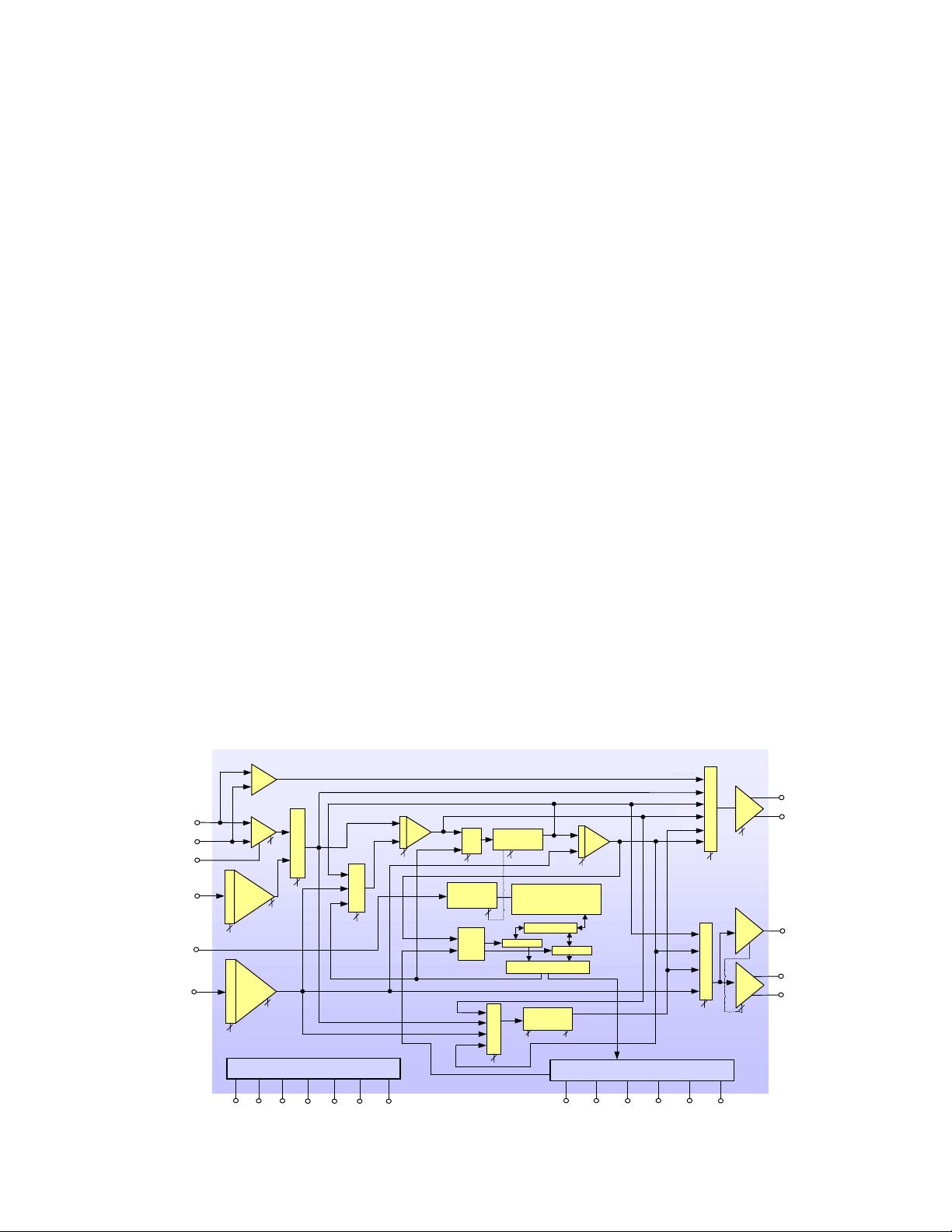
2 Functional Description ...........................................................................................................6
2.1 Internal Registers...............................................................................................................7
2.2 Memory Organization.........................................................................................................7
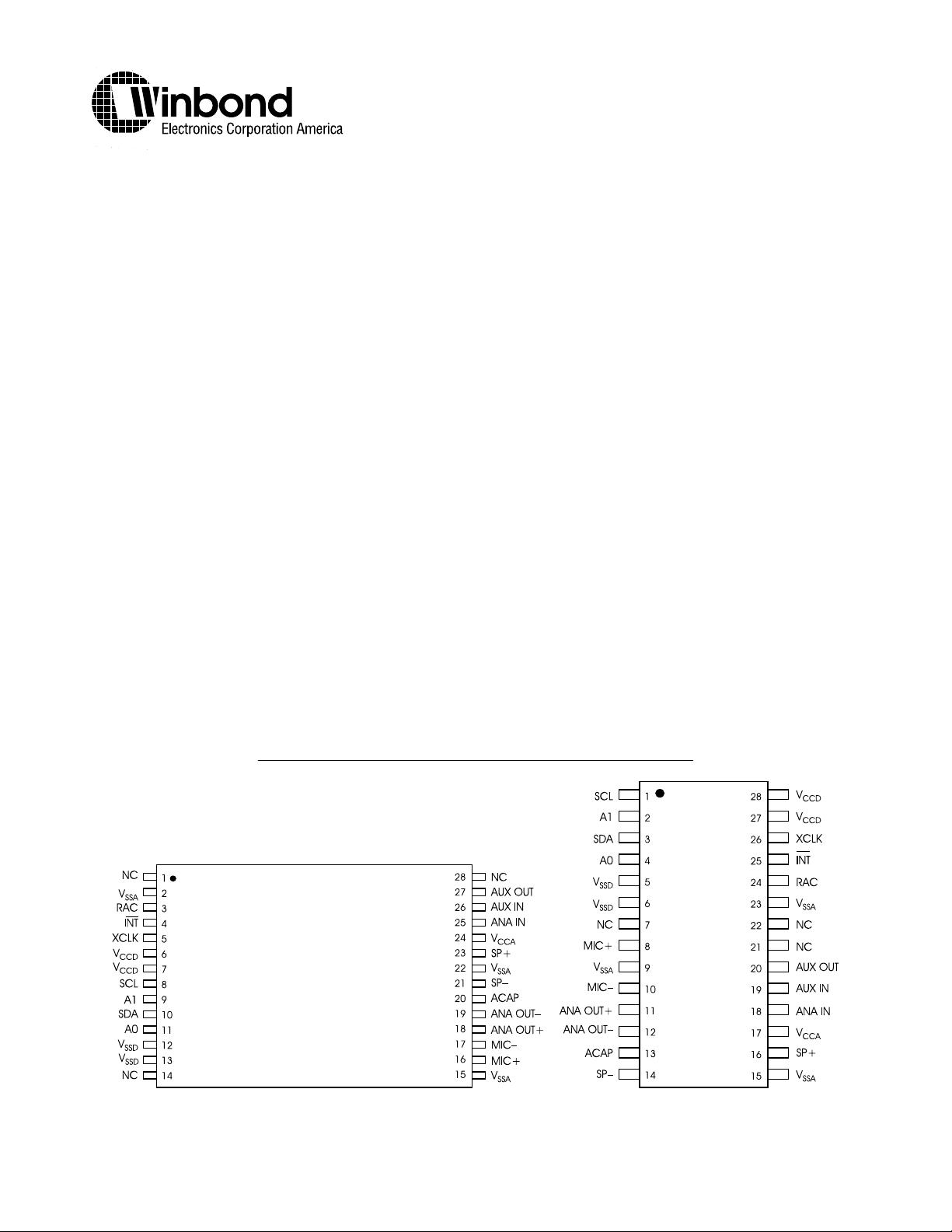
2.3 Pinout Table.......................................................................................................................8
3 Operational Modes Description.............................................................................................9
3.1 I
2
C Interface .......................................................................................................................9
3.2 Command Byte ................................................................................................................11
3.3 Opcode Summary............................................................................................................11
3.4 Data Bytes........................................................................................................................13
3.5 Configuration Register Bytes...........................................................................................13
3.6 Power-up Sequence.........................................................................................................15
3.7 Feed through mMde.........................................................................................................15
3.8 Call Record ......................................................................................................................17
3.9 Memo Record...................................................................................................................18
3.10 Memo and Call Playback.................................................................................................19
3.11 Message Cueing..............................................................................................................20
4 Analog Mode..........................................................................................................................21
4.1 Aux In and Ana In Description.........................................................................................21
4.2 Analog Structure (left half) description.............................................................................22
4.3 Analog Structure (right half) description...........................................................................22
4.4 Volume Control Description.............................................................................................23
4.5 Apeaker and Aux Out Description....................................................................................23
4.6 Ana Out Description.........................................................................................................24
4.7 Analog Inputs...................................................................................................................24
5 Digital Mode...........................................................................................................................27
5.1 Writing Data .....................................................................................................................27
5.2 Reading Data ...................................................................................................................27
5.3 Erasing Data ....................................................................................................................27
5.4 Example Command Sequences ......................................................................................28
6 Pin Descriptions....................................................................................................................31
6.1 Digital I/O Pins .................................................................................................................31
6.2 Analog I/O Pins................................................................................................................33
6.3 Power and Ground Pins...................................................................................................36
6.4 Sample PC Layout...........................................................................................................36
7 Electrical Characteristics and Parameters.........................................................................37
7.1 Electrical Characteristics..................................................................................................37
7.2 Parameters.......................................................................................................................38
8 Timing Diagrams ...................................................................................................................45
8.1 I
2
C Timing Diagram..........................................................................................................45
8.2 Playback and Stop Cycle.................................................................................................45
8.3 Example of Power Up Command (first 12 bits)................................................................46
October 2000 Page 4
9I
2
C Serial Interface Technical Information..........................................................................47
9.1 Characteristics of the I
2
C Serial Interface........................................................................47
9.2 I
2
C Protocol......................................................................................................................49
10 Device Physical Dimensions............................................................................................51
10.1. Plastic Thin Small Outline Package (TSOP) Type e Dimensions................................51
10.2. Plastic Small Outline Integrated Circuit (soic) Dimensions..........................................52
10.3. Plastic Dual Inline Package (PDIP) Dimensions..........................................................53
10.4. Die Bonding Physical Layout........................................................................................54
11 Ordering Information.........................................................................................................56
剩余56页未读,继续阅读
资源评论
天蛾糊
- 粉丝: 279
- 资源: 3
上传资源 快速赚钱
- 我的内容管理 展开
- 我的资源 快来上传第一个资源
- 我的收益 登录查看自己的收益
- 我的积分 登录查看自己的积分
- 我的C币 登录后查看C币余额
- 我的收藏
- 我的下载
- 下载帮助
安全验证
文档复制为VIP权益,开通VIP直接复制
信息提交成功