没有合适的资源?快使用搜索试试~ 我知道了~
资源推荐
资源详情
资源评论
Expert Verilog, SystemVerilog & Synthesis Training
Simulation and Synthesis Techniques for Asynchronous
FIFO Design
Clifford E. Cummings, Sunburst Design, Inc.
cliffc@sunburst-design.com
ABSTRACT
FIFOs are often used to safely pass data from one clock domain to another asynchronous clock domain. Using a
FIFO to pass data from one clock domain to another clock domain requires multi-asynchronous clock design
techniques. There are many ways to design a FIFO wrong. There are many ways to design a FIFO right but still
make it difficult to properly synthesize and analyze the design.
This paper will detail one method that is used to design, synthesize and analyze a safe FIFO between different clock
domains using Gray code pointers that are synchronized into a different clock domain before testing for "FIFO full"
or "FIFO empty" conditions. The fully coded, synthesized and analyzed RTL Verilog model (FIFO Style #1) is
included.
Post-SNUG Editorial Comment
A second FIFO paper by the same author was voted “Best Paper - 1
st
Place” by SNUG attendees, is listed as
reference [3] and is also available for download.
SNUG San Jose 2002 Simulation and Synthesis Techniques for
Rev 1.2 Asynchronous FIFO Design
2
1.0 Introduction
An asynchronous FIFO refers to a FIFO design where data values are written to a FIFO buffer from one clock
domain and the data values are read from the same FIFO buffer from another clock domain, where the two clock
domains are asynchronous to each other.
Asynchronous FIFOs are used to safely pass data from one clock domain to another clock domain.
There are many ways to do asynchronous FIFO design, including many wrong ways. Most incorrectly implemented
FIFO designs still function properly 90% of the time. Most almost-correct FIFO designs function properly 99%+ of
the time. Unfortunately, FIFOs that work properly 99%+ of the time have design flaws that are usually the most
difficult to detect and debug (if you are lucky enough to notice the bug before shipping the product), or the most
costly to diagnose and recall (if the bug is not discovered until the product is in the hands of a dissatisfied
customer).
This paper discusses one FIFO design style and important details that must be considered when doing asynchronous
FIFO design.
The rest of the paper simply refers to an “asynchronous FIFO” as just “FIFO.”
2.0 Passing multiple asynchronous signals
Attempting to synchronize multiple changing signals from one clock domain into a new clock domain and insuring
that all changing signals are synchronized to the same clock cycle in the new clock domain has been shown to be
problematic[1]. FIFOs are used in designs to safely pass multi-bit data words from one clock domain to another.
Data words are placed into a FIFO buffer memory array by control signals in one clock domain, and the data words
are removed from another port of the same FIFO buffer memory array by control signals from a second clock
domain. Conceptually, the task of designing a FIFO with these assumptions seems to be easy.
The difficulty associated with doing FIFO design is related to generating the FIFO pointers and finding a reliable
way to determine full and empty status on the FIFO.
2.1 Synchronous FIFO pointers
For synchronous FIFO design (a FIFO where writes to, and reads from the FIFO buffer are conducted in the same
clock domain), one implementation counts the number of writes to, and reads from the FIFO buffer to increment (on
FIFO write but no read), decrement (on FIFO read but no write) or hold (no writes and reads, or simultaneous write
and read operation) the current fill value of the FIFO buffer. The FIFO is full when the FIFO counter reaches a
predetermined full value and the FIFO is empty when the FIFO counter is zero.
Unfortunately, for asynchronous FIFO design, the increment-decrement FIFO fill counter cannot be used, because
two different and asynchronous clocks would be required to control the counter. To determine full and empty status
for an asynchronous FIFO design, the write and read pointers will have to be compared.
2.2 Asynchronous FIFO pointers
In order to understand FIFO design, one needs to understand how the FIFO pointers work. The write pointer always
points to the next word to be written; therefore, on reset, both pointers are set to zero, which also happens to be the
next FIFO word location to be written. On a FIFO-write operation, the memory location that is pointed to by the
write pointer is written, and then the write pointer is incremented to point to the next location to be written.
Similarly, the read pointer always points to the current FIFO word to be read. Again on reset, both pointers are reset
to zero, the FIFO is empty and the read pointer is pointing to invalid data (because the FIFO is empty and the empty
flag is asserted). As soon as the first data word is written to the FIFO, the write pointer increments, the empty flag is
cleared, and the read pointer that is still addressing the contents of the first FIFO memory word, immediately drives
that first valid word onto the FIFO data output port, to be read by the receiver logic. The fact that the read pointer is
always pointing to the next FIFO word to be read means that the receiver logic does not have to use two clock
periods to read the data word. If the receiver first had to increment the read pointer before reading a FIFO data
SNUG San Jose 2002 Simulation and Synthesis Techniques for
Rev 1.2 Asynchronous FIFO Design
3
word, the receiver would clock once to output the data word from the FIFO, and clock a second time to capture the
data word into the receiver. That would be needlessly inefficient.
The FIFO is empty when the read and write pointers are both equal. This condition happens when both pointers are
reset to zero during a reset operation, or when the read pointer catches up to the write pointer, having read the last
word from the FIFO.
A FIFO is full when the pointers are again equal, that is, when the write pointer has wrapped around and caught up
to the read pointer. This is a problem. The FIFO is either empty or full when the pointers are equal, but which?
One design technique used to distinguish between full and empty is to add an extra bit to each pointer. When the
write pointer increments past the final FIFO address, the write pointer will increment the unused MSB while setting
the rest of the bits back to zero as shown in Figure 1 (the FIFO has wrapped and toggled the pointer MSB). The
same is done with the read pointer. If the MSBs of the two pointers are different, it means that the write pointer has
wrapped one more time that the read pointer. If the MSBs of the two pointers are the same, it means that both
pointers have wrapped the same number of times.
Figure 1 - FIFO full and empty conditions
Using n-bit pointers where (n-1) is the number of address bits required to access the entire FIFO memory buffer, the
FIFO is empty when both pointers, including the MSBs are equal. And the FIFO is full when both pointers, except
the MSBs are equal.
The FIFO design in this paper uses n-bit pointers for a FIFO with 2
(n-1)
write-able locations to help handle full and
empty conditions. More design details related to the full and empty logic are included in section 5.0.
SNUG San Jose 2002 Simulation and Synthesis Techniques for
Rev 1.2 Asynchronous FIFO Design
4
2.3 Binary FIFO pointer considerations
Trying to synchronize a binary count value from one clock domain to another is problematic because every bit of an
n-bit counter can change simultaneously (example 7->8 in binary numbers is 0111->1000, all bits changed). One
approach to the problem is sample and hold periodic binary count values in a holding register and pass a
synchronized ready signal to the new clock domain. When the ready signal is recognized, the receiving clock
domain sends back a synchronized acknowledge signal to the sending clock domain. A sampled pointer must not
change until an acknowledge signal is received from the receiving clock domain. A count-value with multiple
changing bits can be safely transferred to a new clock domain using this technique. Upon receipt of an acknowledge
signal, the sending clock domain has permission to clear the ready signal and re-sample the binary count value.
Using this technique, the binary counter values are sampled periodically and not all of the binary counter values can
be passed to a new clock domain The question is, do we need to be concerned about the case where a binary counter
might continue to increment and overflow or underflow the FIFO between sampled counter values? The answer is
no[8].
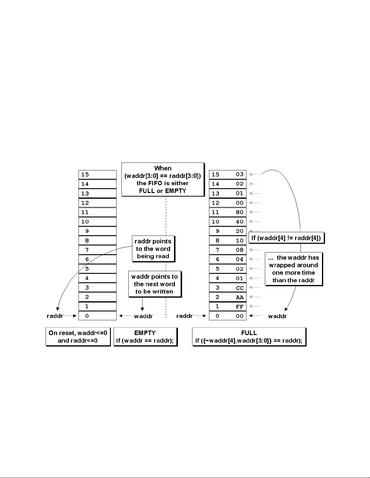
FIFO full occurs when the write pointer catches up to the synchronized and sampled read pointer. The synchronized
and sampled read pointer might not reflect the current value of the actual read pointer but the write pointer will not
try to count beyond the synchronized read pointer value. Overflow will not occur[8].
FIFO empty occurs when the read pointer catches up to the synchronized and sampled write pointer. The
synchronized and sampled write pointer might not reflect the current value of the actual write pointer but the read
pointer will not try to count beyond the synchronized write pointer value. Underflow will not occur[8].More
observations about this technique of sampling binary pointers with a synchronized ready-acknowledge pair of
handshaking signals are detailed in section 7.0, after the discussion of synchronized Gray[6] code pointers.
A common approach to FIFO counter-pointers, is to use Gray code counters. Gray codes only allow one bit to
change for each clock transition, eliminating the problem associated with trying to synchronize multiple changing
signals on the same clock edge.
2.4 FIFO testing troubles
Testing a FIFO design for subtle design problems is nearly impossible to do. The problem is rooted in the fact that
FIFO pointers in an RTL simulation behave ideally, even though, if incorrectly implemented, they can cause
catastrophic failures if used in a real design.
In an RTL simulation, if binary-count FIFO pointers are included in the design all of the FIFO pointer bits will
change simultaneously; there is no chance to observe synchronization and comparison problems. In a gate-level
simulation with no backannotated delays, there is only a slight chance of observing a problem if the gate transitions
are different for rising and falling edge signals, and even then, one would have to get lucky and have the correct
sequence of bits changing just prior to and just after a rising clock edge. For higher speed designs, the delay
differences between rising and falling edge signals diminishes and the probability of detecting problems also
diminishes. Finding actual FIFO design problems is greatest for gate-level designs with backannotated delays, but
even doing this type of simulation, finding problems will be difficult to do and again the odds of observing the
design problems decreases as signal propagation delays diminish.
Clearly the answer is to recognize that there are potential FIFO design problems and to do the design correctly from
the start.
The behavioral model that I sometimes use for testing a FIFO design is a FIFO model that is simple to code, is
accurate for behavioral testing purposes and would be difficult to debug if it were used as an RTL synthesis model.
This FIFO model is only recommended for use in a FIFO testbench. The model accurately determines when FIFO
full and empty status bits should be set and can be used to determine the data values that should have been stored
into a working FIFO. THIS FIFO MODEL IS NOT SAFE FOR SYNTHESIS!
module beh_fifo (rdata, wfull, rempty, wdata,
winc, wclk, wrst_n, rinc, rclk, rrst_n);
SNUG San Jose 2002 Simulation and Synthesis Techniques for
Rev 1.2 Asynchronous FIFO Design
5
parameter DSIZE = 8;
parameter ASIZE = 4;
output [DSIZE-1:0] rdata;
output wfull;
output rempty;
input [DSIZE-1:0] wdata;
input winc, wclk, wrst_n;
input rinc, rclk, rrst_n;
reg [ASIZE:0] wptr, wrptr1, wrptr2, wrptr3;
reg [ASIZE:0] rptr, rwptr1, rwptr2, rwptr3;
parameter MEMDEPTH = 1<<ASIZE;
reg [DSIZE-1:0] ex_mem [0:MEMDEPTH-1];
always @(posedge wclk or negedge wrst_n)
if (!wrst_n) wptr <= 0;
else if (winc && !wfull) begin
ex_mem[wptr[ASIZE-1:0]] <= wdata;
wptr <= wptr+1;
end
always @(posedge wclk or negedge wrst_n)
if (!wrst_n) {wrptr3,wrptr2,wrptr1} <= 0;
else {wrptr3,wrptr2,wrptr1} <= {wrptr2,wrptr1,rptr};
always @(posedge rclk or negedge rrst_n)
if (!rrst_n) rptr <= 0;
else if (rinc && !rempty) rptr <= rptr+1;
always @(posedge rclk or negedge rrst_n)
if (!rrst_n) {rwptr3,rwptr2,rwptr1} <= 0;
else {rwptr3,rwptr2,rwptr1} <= {rwptr2,rwptr1,wptr};
assign rdata = ex_mem[rptr[ASIZE-1:0]];
assign rempty = (rptr == rwptr3);
assign wfull = ((wptr[ASIZE-1:0] == wrptr3[ASIZE-1:0]) &&
(wptr[ASIZE] != wrptr3[ASIZE] ));
endmodule
Example 1 - Behavioral FIFO model for testbench use only - SHOULD NOT BE USED FOR SYNTHESIS!
In the behavioral model of Example 1, it is okay to use binary-count pointers, a Verilog array to represent the FIFO
memory buffer, multi-asynchronous clocks in the same module and non-registered outputs. THIS MODEL IS NOT
INTENDED FOR SYNTHESIS! (Hopefully enough capital letters have been used in this section to discourage
anyone from trying to synthesize this model!)
Two of the always blocks in the module (the always blocks with concatenations) are included to behaviorally
represent the synchronization that will be required in the actual RTL FIFO design. They are not important to the
testing of the data transfer through the FIFO, but they are important to the testing of the correctly timed full and
empty flags in the FIFO model. The exact number of synchronization stages required in the behavioral model is
FIFO-design dependent. This model can be used to help test the FIFO design described in this paper.
剩余22页未读,继续阅读
资源评论
- zhenmafan2014-07-16很不错 值得一读
- Ropeom2013-10-03非常经典的一篇文章!
- franklyfree2013-12-28原来还以为是翻译过来的 ,结果是原版
氧雪冰
- 粉丝: 5
- 资源: 7
上传资源 快速赚钱
- 我的内容管理 展开
- 我的资源 快来上传第一个资源
- 我的收益 登录查看自己的收益
- 我的积分 登录查看自己的积分
- 我的C币 登录后查看C币余额
- 我的收藏
- 我的下载
- 下载帮助
安全验证
文档复制为VIP权益,开通VIP直接复制
信息提交成功