C8051_C2接口说明

Rev. 1.1 12/03 Copyright © 2003 by Silicon Laboratories AN127-DS11
AN127
FLASH PROGRAMMING VIA THE C2 INTERFACE
Relevant Devices
This application note applies to the following devices:
C8051F300, C8051F301, C8051F302, and
C8051F303.
Introduction
This application note describes how to program the
FLASH memory on C8051F30x devices through
the C2 interface. Example software is included.
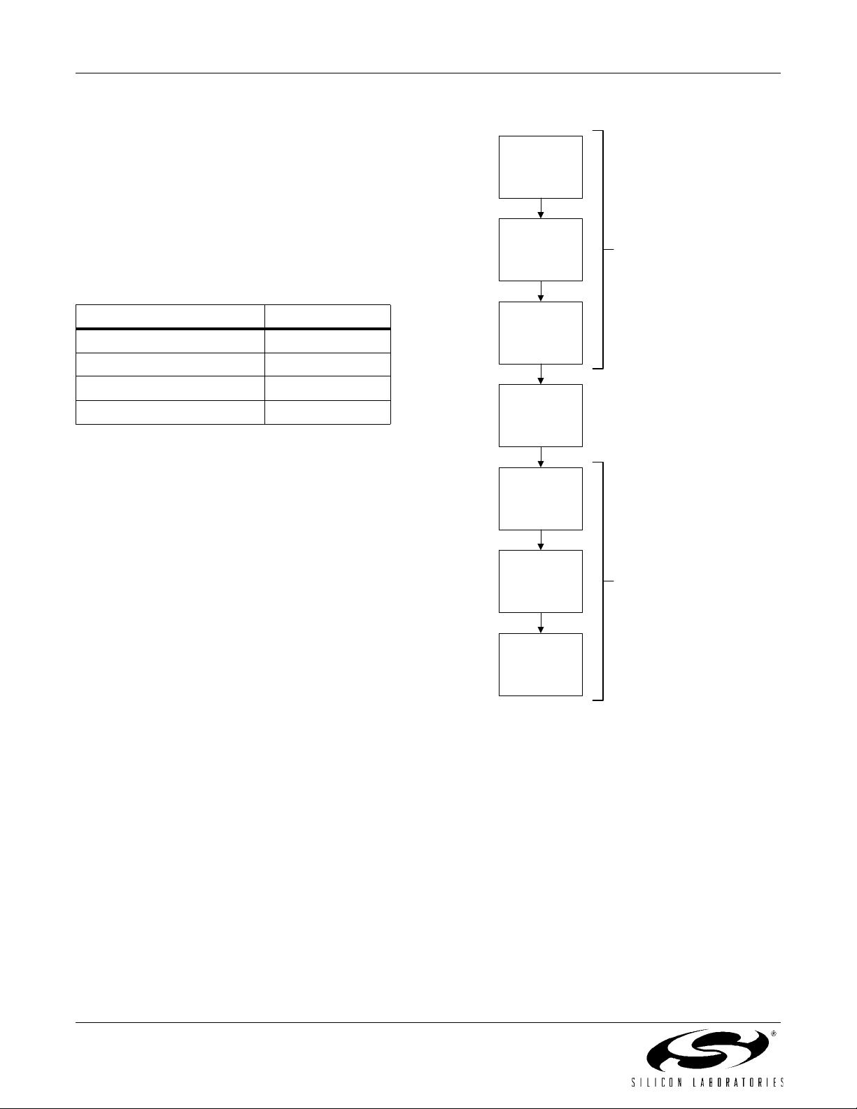
C8051F30x devices have a FLASH Programming
interface (FPI) that is accessed via the C2 Interface
(C2I) and a set of programming registers. The
FLASH access block diagram is shown in Figure 1.
The information needed to access the FLASH
memory via the C2 Interface can be divided into
the three sections listed below.
1. C2 Interface: This includes information about
the C2 physical layer protocol, C2 registers,
and C2 primitive commands.
a. The 2-wire C2 interface (C2CK and
C2D)
b. C2 Address register and its access com-
mands (Address Write, Address Read)
c. C2 Data register access commands
(Data Write, Data Read)
d. Device ID and Revision ID registers
2. FLASH Programming Registers: This
includes the functions of the FLASH Program-
ming registers.
a. FLASH Control register (FPCTL)
b. FLASH Data register (FPDAT)
3. FLASH Programming Interface: This
includes the FLASH Programming Interface
(FPI) commands and procedures.
a. FLASH Block Write
b. FLASH Block Read
c. FLASH Page Erase
d. FLASH User Space Erase
C2 Interface
The C2 Interface (C2I) consists of an Address reg-
ister and access to up to 256 Data registers. Access
to these registers is provided by the C2 physical
layer protocol. For details on the C2 protocol, see
the C2 Specification on the Silicon Labs Applica-
tions website (http://www.silabs.com
).
This application note assumes a basic understand-
ing of the C2 physical layer protocol and the proce-
dure for accessing the C2 Address and Data
registers.
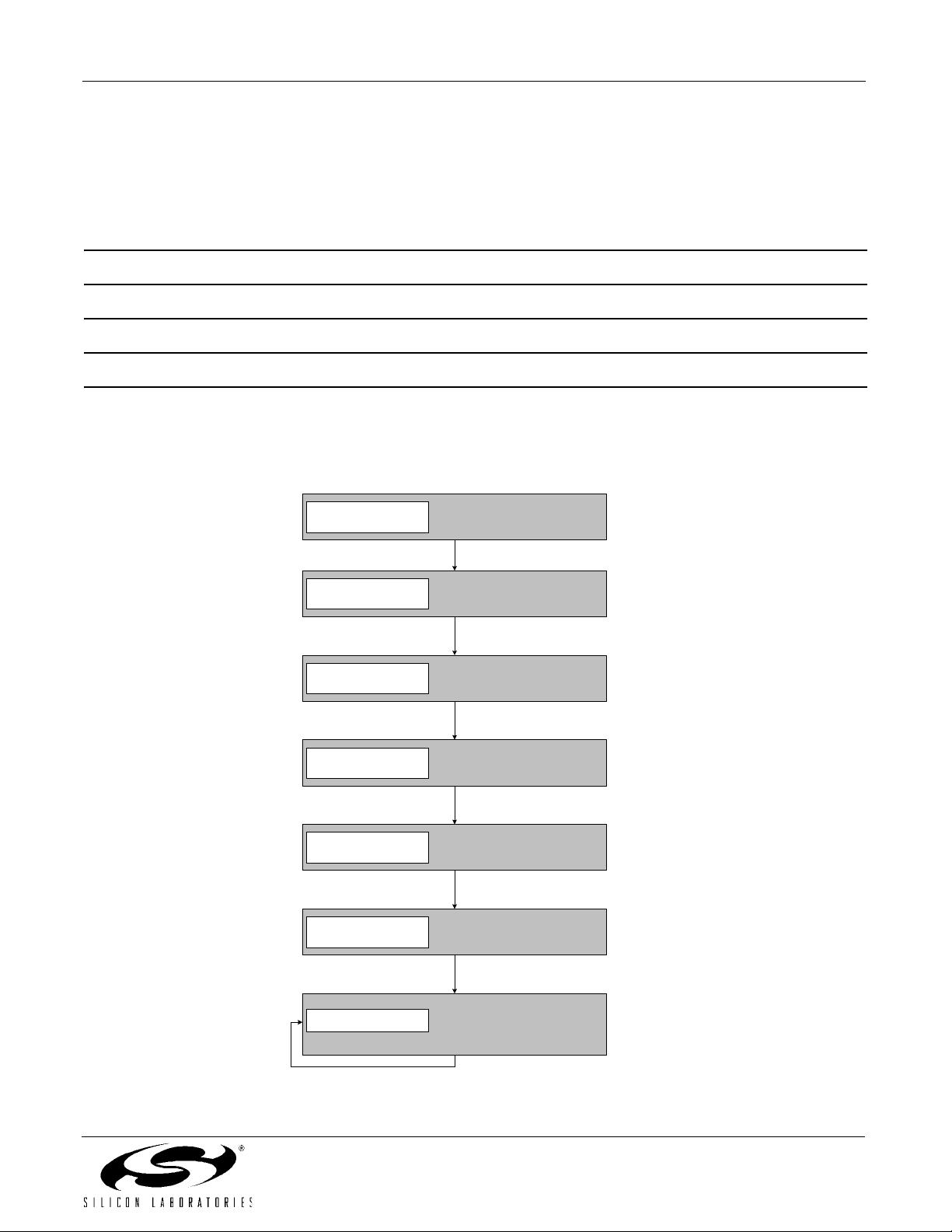
FLASH
Programming
Interface
(FPI)
C2 Interface
(C2I)
FLASH
Programming
Control Register
FLASH
Programming
Data Register
C2CK
C2D
Target Device
Figure 1. C2 FLASH Programming
Architecture
剩余23页未读,继续阅读
资源评论

 yebijiaoman2013-11-17对于我来说挺有用的
- song9152013-04-09参考一下,有用
 「已注销」2018-03-14还是&能管用的,找了一段时间
- lubi199810012014-11-23非常感谢,这资源我找了好久了!
- ahui20092015-02-10还是很管用


