A4950KLJTR-T;中文规格书-Datasheet资料.pdf
需积分: 37 77 浏览量
2019-12-02
00:11:10
上传
评论
收藏 255KB PDF 举报

Description
Designed for pulse width modulated (PWM) control of DC
motors, the A4950 is capable of peak output currents to ±3.5 A
and operating voltages to 40 V.
Input terminals are provided for use in controlling the speed and
direction of a DC motor with externally applied PWM control
signals. Internal synchronous rectification control circuitry is
provided to lower power dissipation during PWM operation.
Internal circuit protection includes overcurrent protection,
motor lead short to ground or supply, thermal shutdown with
hysteresis, undervoltage monitoring of V
BB
, and crossover-
current protection.
For high ambient operating temperature applications, an
automotive grade device is offered (A4950K). The K grade
device is tested across extended temperature and voltage
ranges to ensure compliance in automotive or industrial
applications.
The A4950 is provided in a low-profile 8-pin SOICN package
with exposed thermal pad (suffix LJ) that is lead (Pb) free, with
100% matte tin leadframe plating.
A4950-DS, Rev. 4
Features and Benefits
• Low R
DS(on)
outputs
• Overcurrent protection (OCP)
▫ Motor short protection
▫ Motor lead short to ground protection
▫ Motor lead short to battery protection
• Low Power Standby mode
• Adjustable PWM current limit
• Synchronous rectification
• Internal undervoltage lockout (UVLO)
• Crossover-current protection
• A4950K is AEC-Q100 Grade 1 qualified
• Commercial temperature grade (A4950E: –40°C to 85°C )
• Automotive temperature grade (A4950K: –40°C to 125°C)
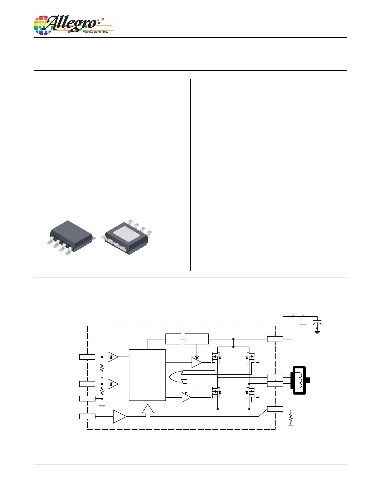
Full-Bridge DMOS PWM Motor Driver
Package: 8-pin SOICN with exposed
thermal pad (suffix LJ)
Functional Block Diagram
Not to scale
A4950
Control
Logic
LSS
OUT1
OUT2
VBB
IN1
IN2
Charge
Pump
OSC
Disable
Load
Supply
UVLO
VREF
7V
GND
÷
(Optional)
TSD
10
http://oneic.com/
资源评论


