AOD4130 60V30A场效应管TO252.pdf
需积分: 2 185 浏览量
2020-12-24
08:45:49
上传
评论
收藏 305KB PDF 举报
AOD4130/AOI4130
60V N-Channel MOSFET
General Description Product Summary
V
DS
I
D
(at V
GS
=10V) 30A
R
DS(ON)
(at V
GS
=10V) < 24mΩ
R
DS(ON)
(at V
GS
=4.5V) < 30mΩ
100% UIS Tested
100% R
g
Tested
Symbol
V
DS
V
GS
I
DM
I
AS
, I
AR
E
AS
, E
AR
T
J
, T
STG
Symbol
t ≤ 10s
Steady-State
Steady-State
R
θJC
Maximum Junction-to-Case
°C/W
°C/W
Maximum Junction-to-Ambient
A D
2.4
50
2.9
Power Dissipation
B
P
D
W
Power Dissipation
A
P
DSM
W
T
A
=70°C
52
1.6
T
A
=25°C
A
T
A
=25°C
I
DSM
A
T
A
=70°C
I
D
30
20
T
C
=25°C
T
C
=100°C
Avalanche energy L=0.1mH
C
mJ
Avalanche Current
C
5
Continuous Drain
Current
36.5
6.5
A27
The AOD4130/AOI4130 combines advanced trench
MOSFET technology with a low resistance package to
provide extremely low R
DS(ON)
. This device is ideal for
boost converters and synchronous rectifiers for
consumer, telecom, industrial power supplies and LED
backlighting.
V
Maximum UnitsParameter
Absolute Maximum Ratings T
A
=25°C unless otherwise noted
60V
V±20Gate-Source Voltage
Drain-Source Voltage 60
Units
Maximum Junction-to-Ambient
A
°C/W
R
θJA
12.4
34
20
Junction and Storage Temperature Range -55 to 175 °C
Thermal Characteristics
74Pulsed Drain Current
C
Continuous Drain
Current
Parameter Typ Max
T
C
=25°C
2.5
25
T
C
=100°C
G
D
S
G
G
D
D
S
S
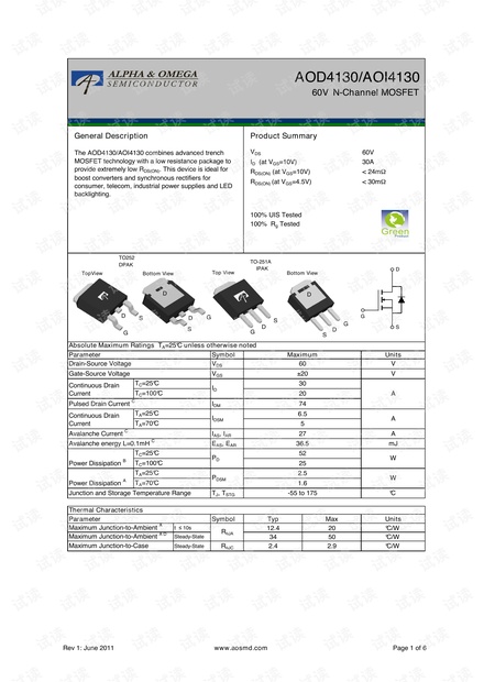
D
Top View
Bottom View
TO-251A
IPAK
TO252
DPAK
TopView
Bottom View
G
G
D
D
S
S
D
Rev 1: June 2011 www.aosmd.com Page 1 of 6


评论0
最新资源