BQ2415-datasheet用户数据手册
需积分: 1 196 浏览量
2018-04-09
14:31:41
上传
评论
收藏 2.29MB PDF 举报

C
VREF
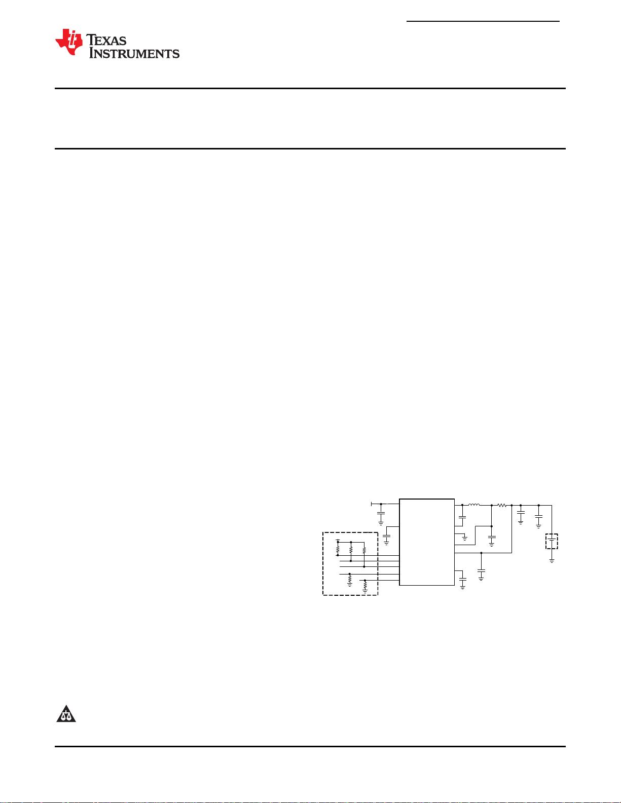
33 nF
C
BOOT
+
PACK–
PACK+
C
CSOUT
SCL
SDA
CSOUT
CSIN
PGND
SW
I
2
C BUS
VAUX
HOST
SCL
SDA
STAT
VREF
STAT
PMID
VBUS
C
IN
V
BUS
C
IN
BOOT
OTG
U1
CD
R
SNS
C
CSIN
V
BAT
1 Fm
4.7 Fm
10 kW
10 kW
L 1.0 H
O
m
C
O1
22 Fm
0.1 Fm
0.1 Fm
1 Fm
bq24157
C
O2
33 Fm
OTG
CD
10 kW
10 kW
10 kW
bq24157
www.ti.com
SLUSB80 –SEPTEMBER 2012
Fully Integrated Switch-Mode Charger
With USB Compliance and USB-OTG Support
Check for Samples: bq24157
1
FEATURES
23
• Power Up System without Battery
• Synchronous Fixed-Frequency PWM
Controller Operating at 3 MHz With 0% to
• Charge Faster than Linear Chargers
99.5% Duty Cycle
• High-Accuracy Voltage and Current Regulation
• Automatic High Impedance Mode for Low
– Input Current Regulation Accuracy: ±5%
Power Consumption
(100 mA and 500 mA)
• Robust Protection
– Charge Voltage Regulation Accuracy:
– Reverse Leakage Protection Prevents
±0.5% (25°C), ±1% (0°C to 125°C)
Battery Drainage
– Charge Current Regulation Accuracy: ±5%
– Thermal Regulation and Protection
• Input Voltage Based Dynamic Power
– Input/Output Overvoltage Protection
Management (VIN DPM)
• Status Output for Charging and Faults
• Bad Adaptor Detection and Rejection
• USB Friendly Boot-Up Sequence
• Safety Limit Register for Maximum Charge
Voltage and Current Limiting • Automatic Charging
• High-Efficiency Mini-USB/AC Battery Charger • Boost Mode Operation for USB OTG
for Single-Cell Li-Ion and Li-Polymer Battery
– Input Voltage Range (from Battery): 3.2 V to
Packs
4.5 V
• 20-V Absolute Maximum Input Voltage Rating
• 2.1 mm x 2 mm 20-Pin WCSP Package
• 6.5-V Maximum Operating Input Voltage
APPLICATIONS
• Built-In Input Current Sensing and Limiting
• Mobile and Smart Phones
• Integrated Power FETs for Up To 1.25-A
Charge Rate
• MP3 Players
• Programmable Charge Parameters through
• Handheld Devices
I
2
C™ Compatible Interface (up to 3.4 Mbps):
Figure 1. Typical Application Circuit
– Input Current Limit
– VIN DPM Threshold
– Fast-Charge/Termination Current
– Charge Regulation Voltage (3.5 V to 4.44 V)
– Low Charge Current Mode Enable/Disable
– Termination Enable/Disable
1
Please be aware that an important notice concerning availability, standard warranty, and use in critical applications of
Texas Instruments semiconductor products and disclaimers thereto appears at the end of this data sheet.
2NanoFree is a trademark of Texas Instruments.
3I
2
C is a trademark of NXP B.V. Corporation.
PRODUCTION DATA information is current as of publication date.
Copyright © 2012, Texas Instruments Incorporated
Products conform to specifications per the terms of the Texas
Instruments standard warranty. Production processing does not
necessarily include testing of all parameters.
捷多邦,您值得信赖的PCB打样专家!

剩余38页未读,继续阅读
资源评论


萧承影
- 粉丝: 1
- 资源: 1


最新资源
- AIS2024 valid
- 最入门的爬虫代码 python.docx
- 爬虫零基础入门-爬取天气预报.pdf
- 最通俗易懂的 MongoDB 非结构化文档存储数据库教程.zip
- 以mongodb为数据库的订单物流小项目.zip
- 腾讯云-mongodb数据库, 项目部署.zip
- 腾讯 APIJSON 的 MongoDB 数据库插件.zip
- 理解非关系型数据库和关系型数据库的区别.zip
- 操作简单的Mongodb网页web管理工具,基于Spring Boot2.0支持mongodb集群.zip
- tms-mongodb-web,提供访问mongodb数据的REST API和可灵活扩展的mongodb web 客户端.zip
资源上传下载、课程学习等过程中有任何疑问或建议,欢迎提出宝贵意见哦~我们会及时处理!
点击此处反馈


