没有合适的资源?快使用搜索试试~ 我知道了~
资源推荐
资源详情
资源评论
COMPANY CONFIDENTIAL • 1
Data Sheet
© 2010 by Atheros Communications, Inc. All rights reserved. Atheros®, Atheros Driven®, Align®, Atheros XR®, Driving the Wireless Future®, Intellon®, No New Wires®,
Orion® , PLC4Trucks®, Powerpacket®, Spread Spectrum Carrier®, SSC®, ROCm®, Super A/G®, Super G®, Super N®, The Air is Cleaner at 5-GHz®, Total 802.11®, U-
Nav®, Wake on Wireless®, Wireless Future. Unleashed Now.®, and XSPAN®, are registered by Atheros Communications, Inc. Atheros SST™, Signal-Sustain Technology™,
Ethos™, Install N Go™, IQUE™, ROCm™, amp™, Simpli-Fi™, There is Here™, U-Map™, U-Tag™, and 5-UP™ are trademarks of Atheros Communications, Inc. The
Atheros logo is a registered trademark of Atheros Communications, Inc. All other trademarks are the property of their respective holders. Subject to change without notice.
PRELIMINARY
December 2010
AR9331 Highly-Integrated and Cost Effective IEEE 802.11n
1x1 2.4 GHz SoC for AP and Router Platforms
General Description
The Atheros AR9331 is a highly integrated and
cost effective IEEE 802.11n 1x1 2.4 GHz System-
on-a-Chip (SoC) for wireless local area network
(WLAN) AP and router platforms.
In a single chip, the AR9331 includes a MIPS 24K
processor, five-port IEEE 802.3 Fast Ethernet
Switch with MAC/PHY, one USB 2.0 MAC/PHY,
and external memory interface for serial Flash,
SDRAM, DDR1 or DDR2, I
2
S/SPDIF-Out audio
interface, SLIC VOIP/PCM interface, UART, and
GPIOs that can be used for LED controls or other
general purpose interface configurations.
The AR9331 integrates two Gbit MACs plus a
five-port Fast Ethernet switch with a four-traffic
class Quality of Service (QoS) engine.
The AR9331 integrates an 802.11n 1x1 MAC/BB/
radio with internal PA and LNA. It supports
802.11n operations up to 72 Mbps for 20 MHz
and 150 Mbps for 40 MHz channel respectively,
and IEEE 802.11b/g data rates. Additional
features include on-chip one-time programmable
(OTP) memory.
Features
■ Complete IEEE 802.11n 1x1 AP or router in a
single chip
■ MIPS 24K processor operating at up to
400 MHz
■ External 16-bit DDR1, DDR2, or SDRAM
memory interface
■ SPI NOR Flash memory support
■ No external EEPROM needed
■ 4 LAN ports and 1 WAN port IEEE 802.3 Fast
Ethernet switch with auto-crossover, auto
polarity, and auto-negotiation in PHYs
■ Four classes of QoS per port
■ Fully integrated RF front-end including PA
and LNA
■ Optional external LNA/PA
■ Switched antenna diversity
■ High-speed UART for console support
■ I
2
S/SPDIF-out audio interface
■ SLIC for VOIP/PCM
■ USB 2.0 host/device mode support
■ GPIO/LED support
■ JTAG-based processor debugging supported
■ 25 MHz or 40 MHz reference clock input
■ Advanced power management with dynamic
clock switching for ultra-low power modes
■ 148-pin, 12 mm x 12 mm dual-row LPCC
package
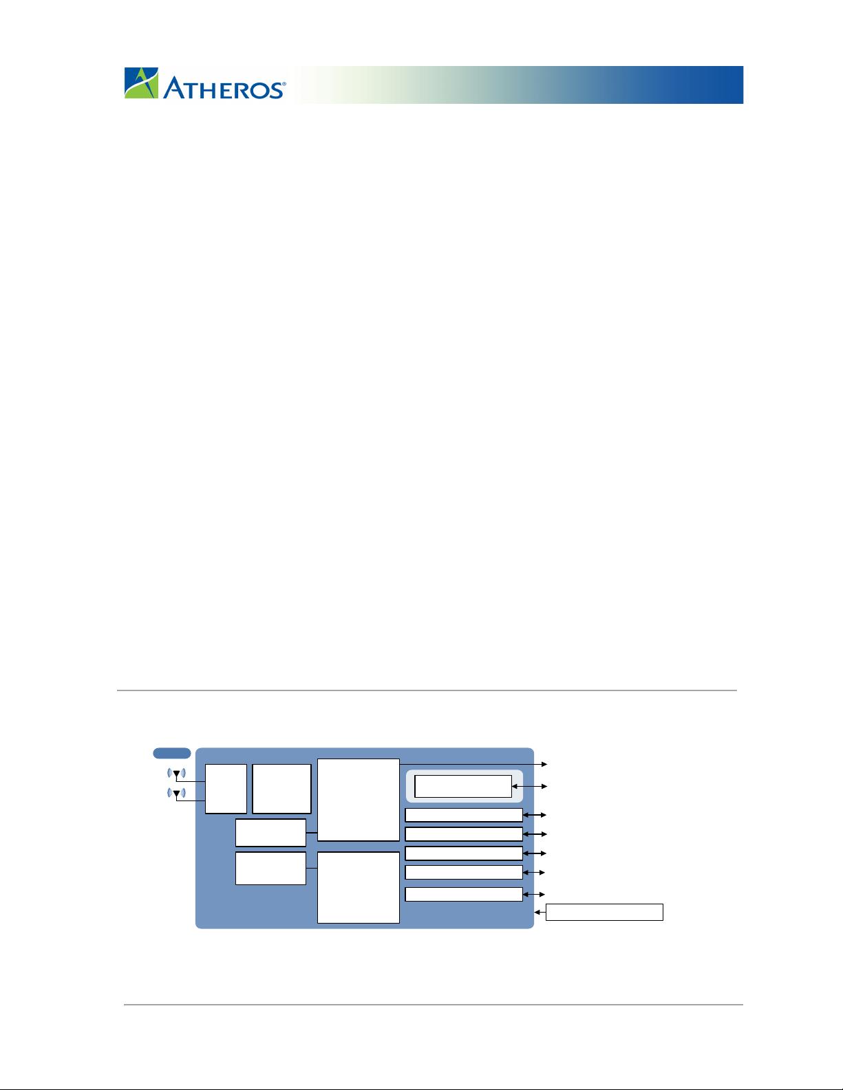
System Block Diagram
SDRAM/
DDR1/DDR2
Controller and
NOR Flash
Memory
Interface
MIPS 24K
Processor
AR9331
Serial Flash and SDRAM/DDR Interface
USB MAC/PHY USB 2.0 Interface
5x Fast Ethernet
LAN/WAN Ports
5x Fast Ethernet Ports
External Interface GPIOs/LEDs
UART UART Interface
2.4 G Hz
802.11n
1x1 WLAN
MAC/BB/
Radio
RF
Front
End
25 or 40 MHz Crystal
I
2
S/SPDIF Au dio Interf ace
Internal
SRAM
I- Cache
D-Cache
SLIC VOIP/PCM
PRELIMINARY
2 • AR9331 802.11n 1x1 2.4 GHz SoC for AP and Router Platforms Atheros Communications, Inc.
2 • December 2010 COMPANY CONFIDENTIAL
PRELIMINARY
Atheros Communications, Inc. AR9331 802.11n 1x1 2.4 GHz SoC for AP and Router Platforms • 1
COMPANY CONFIDENTIAL December 2010 • 1
Table of Contents
1 Pin Descriptions .......................... 13
2 Functional Description ............... 21
2.1 MIPS Processor ....................................... 22
2.2 Configuration ......................................... 22
2.3 AR9331 Address MAP .......................... 23
2.4 AHB Master Bus ..................................... 23
2.5 APB Bridge .............................................. 23
2.6 DDR Memory Controller ...................... 23
2.7 Serial Flash (SPI) .................................... 24
2.8 UART ....................................................... 24
2.9 GE0 and GE1 ........................................... 25
2.10 MDC/MDIO Interface ......................... 25
2.11 Ethernet Switch Controller .................. 26
2.11.1 VLANs For LAN Ports ............... 28
2.11.2 Quality of Service (QoS) for LAN
Ports .............................................. 29
2.12 Rate Limiting ......................................... 29
2.13 Broadcast Storm Control ...................... 30
2.14 Switch Operation .................................. 30
2.15 Port Mirroring ....................................... 30
2.16 Port States ............................................... 30
3 Medium Access Control (MAC) 31
3.1 Overview ................................................. 31
3.2 Descriptor ................................................ 31
3.3 Descriptor Format .................................. 32
3.4 Queue Control Unit (QCU) .................. 47
3.5 DCF Control Unit (DCU) ...................... 47
3.5.1 DCU State Information .............. 48
3.6 Protocol Control Unit (PCU) ................ 48
4 Digital PHY Block ....................... 49
4.1 Overview ................................................. 49
4.2 802.11n Mode .......................................... 49
4.2.1 Transmitter (Tx) .......................... 49
4.2.2 Receiver (Rx) ............................... 49
4.3 802.11b/g Legacy Mode ........................ 50
4.3.1 Transmitter .................................. 50
4.3.2 Receiver ........................................ 50
5 Radio Block ...................................51
5.1 Receiver (Rx) Block ................................ 51
5.2 Transmitter (Tx) Block .......................... 51
5.3 Synthesizer (SYNTH) Block ................. 52
5.4 Bias/Control (BIAS) Block ................... 52
6 Register Descriptions ..................53
6.1 DDR Registers ........................................ 54
6.1.1 DRR DRAM Configuration
(DDR_CONFIG) ......................... 54
6.1.2 DDR DRAM Configuration 2
(DDR_CONFIG2) ....................... 55
6.1.3 DDR Mode Value
(DDR_MODE_REGISTER) ........ 55
6.1.4 DDR Extended Mode
(DDR_EXTENDED_MODE_REGIS
TER) .............................................. 55
6.1.5 DDR Control (DDR_CONTROL) 56
6.1.6 DDR Refresh Control and
Configuration (DDR_REFRESH) 56
6.1.7 DDR Read Data Capture Bit Mask
(DDR_RD_DATA_THIS_CYCLE)
56
6.1.8 DQS Delay Tap Control for Byte 0
(TAP_CONTROL_0) .................. 56
6.1.9 DQS Delay Tap Control for Byte 1
(TAP_CONTROL_1) .................. 57
6.1.10 GE0 Interface Write Buffer Flush
(DDR_WB_FLUSH_GE0) .......... 57
6.1.11 GE1 Interface Write Buffer Flush
(DDR_WB_FLUSH_GE1) .......... 57
6.1.12 USB Interface Write Buffer Flush
(DDR_WB_FLUSH_USB) .......... 57
6.1.13 AMBA Interface Write Buffer Flush
(DDR_WB_FLUSH_AMBA) ..... 58
6.1.14 DDR2 Configuration
(DDR_DDR2_CONFIG) ............. 58
6.1.15 DDR EMR2 (DDR_EMR2) ......... 58
6.1.16 DDR EMR3 (DDR_EMR3) ......... 58
6.1.17 DDR Burst Control (DDR_BURST)
59
6.1.18 AHB Master Timeout Control
(AHB_MASTER_TIMEOUT_MAX)
....................................................... 59
6.1.19 AHB Timeout Current Count
PRELIMINARY
2 • AR9331 802.11n 1x1 2.4 GHz SoC for AP and Router Platforms Atheros Communications, Inc.
2 • December 2010 COMPANY CONFIDENTIAL
(AHB_MASTER_TIMEOUT_CUR
NT) ................................................ 59
6.1.20 Timeout Slave Address
(AHB_MASTER_TIMEOUT_SLV_
ADDR) .......................................... 59
6.2 UART Registers ...................................... 60
6.2.1 UART Transmit and Rx FIFO
Interface (UART_DATA) ........... 60
6.2.2 UART Configuration and Status
(UART_CS) .................................. 61
6.2.3 UART Clock (UART_CLOCK) . 62
6.2.4 UART Interrupt/Control Status
(UART_INT) ................................ 62
6.2.5 UART Interrupt Enable
(UART_INT_EN) ........................ 63
6.3 USB Registers ..........................................64
6.3.1 USB Power Control and Status
(USBPWRCTL) ............................64
6.3.2 USB Configuration
(USB_CONFIG) ........................... 64
6.4 GPIO Registers ....................................... 65
6.4.1 General Purpose I/O Output
Enable (GPIO_OE) ......................65
6.4.2 General Purpose I/O Input Value
(GPIO_IN) .................................... 65
6.4.3 General Purpose I/O Output Value
(GPIO_OUT) ................................ 65
6.4.4 General Purpose I/O Per Bit Set
(GPIO_SET) ................................. 66
6.4.5 General Purpose I/O Per Bit Clear
(GPIO_CLEAR) ........................... 66
6.4.6 General Purpose I/O Interrupt
Enable (GPIO_INT) .................... 66
6.4.7 General Purpose I/O Interrupt
Type (GPIO_INT_TYPE) ........... 66
6.4.8 General Purpose I/O Interrupt
Polarity (GPIO_INT_POLARITY)
66
6.4.9 General Purpose I/O Interrupt
Pending (GPIO_INT_PENDING) .
67
6.4.10 General Purpose I/O Interrupt
Mask (GPIO_INT_MASK) ......... 67
6.4.11 General Purpose I/O Function
(GPIO_FUNCTION_1) ............... 67
6.4.12 General Purpose I/O Input Value
(GPIO_IN_ETH_SWITCH_LED) 68
6.4.13 Extended GPIO Function Control
(GPIO_FUNCTION_2) .............. 69
6.5 PLL Control Registers ........................... 70
6.5.1 CPU Phase Lock Loop
Configuration
(CPU_PLL_CONFIG) ................. 70
6.5.2 CPU Phase Lock Loop
Configuration Register 2
(CPU_PLL_CONFIG2) ............... 70
6.5.3 CPU Clock Control Register
(CLOCK_CONTROL) ................ 71
6.5.4 CPU PLL Dither FRAC Register
(PLL_DITHER_FRAC) ............... 71
6.5.5 CPU PLL Dither Register
(PLL_DITHER) ............................ 72
6.5.6 Ethernet Switch Clock Control
Register (ETHSW_CLOCK
CONTROL) .................................. 72
6.5.7 Ethernet XMII Control Register
(ETH_XMII_CONTROL) ........... 73
6.5.8 Suspend Register (SUSPEND) .. 73
6.5.9 WLAN Clock Control Register
(WLAN_CLOCK_CONTROL) . 74
6.6 Reset Control Registers ......................... 75
6.6.1 General Purpose Timers
(RST_GENERAL_TIMER) ......... 75
6.6.2 General Purpose Timers Reload
(RST_GENERAL_TIMER_RELOA
D) .................................................. 75
6.6.3 Watchdog Timer Control Register
(RST_WATCHDOG_TIMER_CON
TROL) ........................................... 76
6.6.4 Watchdog Timer Register
(RST_WATCHDOG_TIMER) ... 76
6.6.5 Miscellaneous Interrupt Status
(RST_MISC_INTERRUPT_STATUS
) ...................................................... 77
6.6.6 Miscellaneous Interrupt Mask
(RST_MISC_INTERRUPT_MASK)
78
6.6.7 Global Interrupt Status
(RST_GLOBAL_INTERRUPT_STA
TUS) .............................................. 79
6.6.8 Reset (RST_RESET) .................... 80
6.6.9 Chip Revision ID
(RST_REVISION_ID) ................. 80
6.6.10 Bootstrap Status (BOOT_STRAP)
81
PRELIMINARY
Atheros Communications, Inc. AR9331 802.11n 1x1 2.4 GHz SoC for AP and Router Platforms • 3
COMPANY CONFIDENTIAL December 2010 • 3
6.6.11 USB PHY Reset Control
(USB_PHY_RESET) .................... 82
6.7 GMAC Register ......................................83
6.7.1 Ethernet Configuration
(ETH_CFG) .................................. 83
6.8 SLIC Registers ........................................ 84
6.8.1 SLIC Slots Register (SLIC_SLOT) 84
6.8.2 SLIC Clock Control Register
(SLIC_CLOCK_CONTROL) ..... 84
6.8.3 SLIC Control Register
(SLIC_CTRL) ............................... 85
6.8.4 SLIC Tx Slots 1 Register
(SLIC_TX_SLOTS1) .................... 85
6.8.5 SLIC Tx Slots 2 Register
(SLIC_TX_SLOTS2) .................... 85
6.8.6 SLIC Rx Slots 1 Register
(SLIC_RX_SLOTS1) .................... 85
6.8.7 SLIC Rx Slots 2 Register
(SLIC_RX_SLOTS2) .................... 86
6.8.8 SLIC Timing Control Register
(SLIC_TIMING_CTRL) .............. 86
6.8.9 SLIC Interrupt Register
(SLIC_INTR) ................................ 86
6.8.10 SLIC Swap Register (SLIC_SWAP)
87
6.9 MBOX Registers ..................................... 88
6.9.1 Non-Destructive FIFO Status Query
(MBOX_FIFO_STATUS) ............ 88
6.9.2 Non-Destructive SLIC FIFO Status
Query
(SLIC_MBOX_FIFO_STATUS) . 89
6.9.3 Mailbox DMA Engine Policy
Control (MBOX_DMA_POLICY) 89
6.9.4 SLIC Mailbox DMA Engine Policy
Control
(SLIC_MBOX_DMA_POLICY) . 90
6.9.5 Mailbox Rx DMA Descriptors Base
Address
(MBOX_DMA_RX_DESCRIPTOR_
BASE) ............................................ 90
6.9.6 Mailbox Rx DMA Control
(MBOX_DMA_RX_CONTROL) 91
6.9.7 Mailbox Tx DMA Descriptors Base
Address
(MBOX_DMA_TX_DESCRIPTOR_
BASE) ............................................ 91
6.9.8 Mailbox Tx DMA Control
(MBOX_DMA_TX_CONTROL) 92
6.9.9 SLIC Mailbox Rx DMA Descriptors
Base Address
(SLIC_MBOX_DMA_RX_DESCRIP
TOR_BASE) ................................. 92
6.9.10 SLIC Mailbox Rx DMA Control
(SLIC_MBOX_DMA_RX_CONTRO
L) ................................................... 93
6.9.11 SLIC Mailbox Tx DMA Descriptors
Base Address
(SLIC_MBOX_DMA_TX_DESCRIP
TOR_BASE) ................................. 93
6.9.12 SLIC Mailbox Tx DMA Control
(SLIC_MBOX_DMA_TX_CONTRO
L) ................................................... 94
6.9.13 Mailbox FIFO Status
(MBOX_FRAME) ........................ 94
6.9.14 SLIC Mailbox FIFO Status
(SLIC_MBOX_FRAME) ............. 94
6.9.15 FIFO Timeout Period
(FIFO_TIMEOUT) ...................... 95
6.9.16 MBOX Related Interrupt Status
(MBOX_INT_STATUS) .............. 95
6.9.17 SLIC MBOX Related Interrupt
Status
(SLIC_MBOX_INT_STATUS) ... 96
6.9.18 MBOX Related Interrupt Enables
(MBOX_INT_ENABLE) ............. 96
6.9.19 SLIC MBOX Related Interrupt
Enables
(SLIC_MBOX_INT_ENABLE) .. 97
6.9.20 Reset and Clear MBOX FIFOs
(MBOX_FIFO_RESET) ............... 97
6.9.21 SLIC Reset and Clear MBOX FIFOs
(SLIC_MBOX_FIFO_RESET) .... 97
6.10 I
2
S Registers ........................................... 98
6.10.1 Configure Stereo Block
(STEREO0_CONFIG) ................. 98
6.10.2 Set Stereo Volume
(STEREO0_VOLUME) ............. 100
6.10.3 Tx Sample Counter
(STEREO0_TX_SAMPLE_CNT_LS
B) ................................................. 101
6.10.4 Tx Sample Counter
(STEREO0_TX_SAMPLE_CNT_MS
B) ................................................. 101
6.10.5 Rx Sample Counter
(STEREO0_RX_SAMPLE_CNT_LS
B) ................................................. 101
6.10.6 Stereo Clock Divider
剩余319页未读,继续阅读
资源评论
- yaoshuangaa2015-04-17很好 正需要这个 再看看
- moonfishsky2015-09-21在这找规格书很方便,非常感谢
- jixin_w2016-05-23这个规格书和最新差别不是很大,可以参考
- gale3202015-07-07不是最新的,但是没多大问题。
qq183326061
- 粉丝: 0
- 资源: 2
上传资源 快速赚钱
- 我的内容管理 展开
- 我的资源 快来上传第一个资源
- 我的收益 登录查看自己的收益
- 我的积分 登录查看自己的积分
- 我的C币 登录后查看C币余额
- 我的收藏
- 我的下载
- 下载帮助
安全验证
文档复制为VIP权益,开通VIP直接复制
信息提交成功