没有合适的资源?快使用搜索试试~ 我知道了~
资源推荐
资源详情
资源评论
TMS320VC5409
FIXED-POINT DIGITAL SIGNAL PROCESSOR
SPRS082A – APRIL 1999 – REVISED JUNE 1999
1
POST OFFICE BOX 1443 • HOUSTON, TEXAS 77251–1443
D
Advanced Multibus Architecture With Three
Separate 16-Bit Data Memory Buses and
One Program Memory Bus
D
40-Bit Arithmetic Logic Unit (ALU),
Including a 40-Bit Barrel Shifter and Two
Independent 40-Bit Accumulators
D
17- × 17-Bit Parallel Multiplier Coupled to a
40-Bit Dedicated Adder for Non-Pipelined
Single-Cycle Multiply/Accumulate (MAC)
Operation
D
Compare, Select, and Store Unit (CSSU) for
the Add/Compare Selection of the Viterbi
Operator
D
Exponent Encoder to Compute an
Exponent Value of a 40-Bit Accumulator
Value in a Single Cycle
D
Two Address Generators With Eight
Auxiliary Registers and Two Auxiliary
Register Arithmetic Units (ARAUs)
D
Data Bus With a Bus-Holder Feature
D
Extended Addressing Mode for 8M × 16-Bit
Maximum Addressable External Program
Space
D
16K x 16-Bit On-Chip ROM
D
32K x 16-Bit Dual-Access On-Chip RAM
D
Single-Instruction-Repeat and
Block-Repeat Operations for Program Code
D
Block-Memory-Move Instructions for Better
Program and Data Management
D
Instructions With a 32-Bit Long Word
Operand
D
Instructions With Two- or Three-Operand
Reads
D
Arithmetic Instructions With Parallel Store
and Parallel Load
D
Conditional Store Instructions
D
Fast Return From Interrupt
D
On-Chip Peripherals
– Software-Programmable Wait-State
Generator and Programmable Bank
Switching
– On-Chip Phase-Locked Loop (PLL) Clock
Generator With Internal Oscillator or
External Clock Source
– Three Multichannel Buffered Serial Ports
(McBSPs)
– Enhanced 8-Bit Parallel Host-Port
Interface With 16-Bit Data/Addressing
– One 16-Bit Timer
– Six-Channel Direct Memory Access
(DMA) Controller
D
Power Consumption Control With IDLE1,
IDLE2, and IDLE3 Instructions With
Power-Down Modes
D
CLKOUT Off Control to Disable CLKOUT
D
On-Chip Scan-Based Emulation Logic,
IEEE Std 1149.1
†
(JTAG) Boundary Scan
Logic
D
10-ns Single-Cycle Fixed-Point Instruction
Execution Time (100 MIPS) for 3.3-V Power
Supply (1.8-V Core)
D
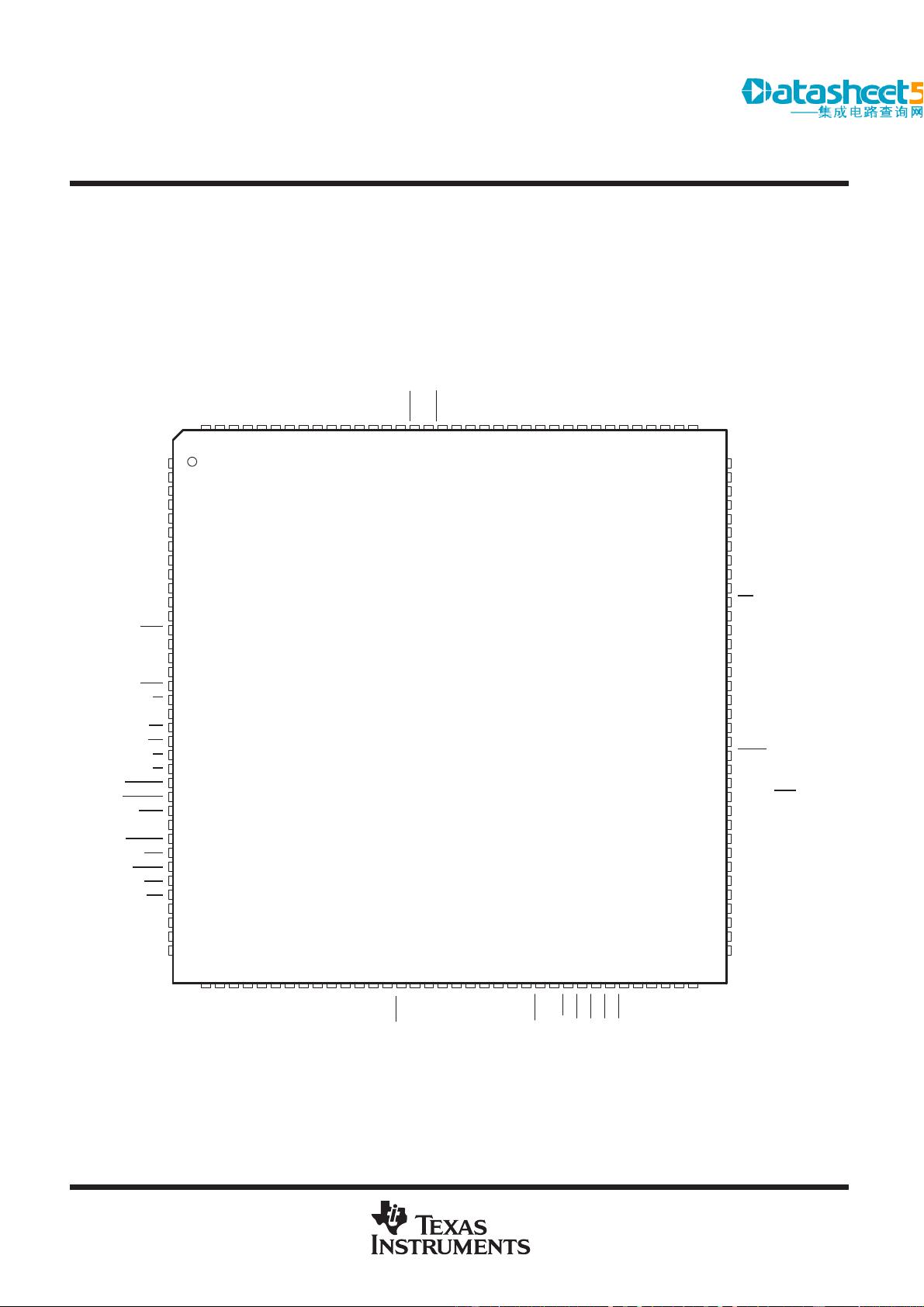
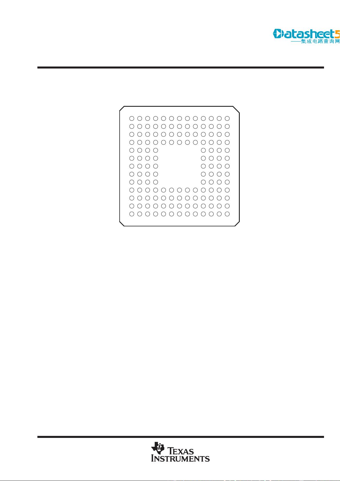
Available in a 144-Pin Plastic Thin Quad
Flatpack (TQFP) (PGE Suffix) and a 144-Pin
Ball Grid Array (BGA) (GGU Suffix)
description
The TMS320VC5409 fixed-point, digital signal processor (DSP) (hereafter referred to as the ’5409 unless
otherwise specified) is based on an advanced modified Harvard architecture that has one program memory bus
and three data memory buses. This processor provides an arithmetic logic unit (ALU) with a high degree of
parallelism, application-specific hardware logic, on-chip memory, and additional on-chip peripherals. The basis
of the operational flexibility and speed of this DSP is a highly specialized instruction set.
Separate program and data spaces allow simultaneous access to program instructions and data, providing the
high degree of parallelism. Two read operations and one write operation can be performed in a single cycle.
Instructions with parallel store and application-specific instructions can fully utilize this architecture. In addition,
Please be aware that an important notice concerning availability, standard warranty, and use in critical applications of
Texas Instruments semiconductor products and disclaimers thereto appears at the end of this data sheet.
ADVANCE INFORMATION
Copyright 1999, Texas Instruments Incorporated
†
IEEE Standard 1149.1-1990 Standard-Test-Access Port and Boundary Scan Architecture.
ADVANCE INFORMATION concerns new products in the sampling or
preproduction phase of development. Characteristic data and other
specifications are subject to change without notice.
TMS320VC5409
FIXED-POINT DIGITAL SIGNAL PROCESSOR
SPRS082A – APRIL 1999 – REVISED JUNE 1999
2
POST OFFICE BOX 1443 • HOUSTON, TEXAS 77251–1443
description (continued)
data can be transferred between data and program spaces. Such parallelism supports a powerful set of
arithmetic, logic, and bit-manipulation operations that can all be performed in a single machine cycle. In addition,
the ’5409 includes the control mechanisms to manage interrupts, repeated operations, and function calls.
For detailed information on the architecture of the ’C5000 family of DSPs, see the
TMS320C5000 DSP Family
Functional Overview
(literature number SPRU307).
CV
HDS1
A18
A17
V
SS
A16
D5
D4
D3
D2
D1
D0
RS
X2/CLKIN
X1
HD3
CLKOUT
V
SS
HPIENA
CV
DD
V
SS
TMS
TCK
TRST
TDI
TDO
EMU1/OFF
EMU0
TOUT
HD2
HPI16
CLKMD3
CLKMD2
CLKMD1
V
SS
DV
DD
BDX1
BFSX1
V
SS
A22
V
SS
DV
DD
A10
HD7
A11
A12
A13
A14
A15
CV
DD
HAS
V
SS
V
SS
CV
DD
HCS
HR/W
READY
PS
DS
IS
R/W
MSTRB
IOSTRB
MSC
XF
HOLDA
IAQ
HOLD
BIO
MP/MC
DV
DD
V
SS
BDR1
BFSR1
144
A21
CV
143
142
141
A8
140
A7
139
A6
138
A5
137
A4
136
HD6
135
A3
134
A2
133
A1
132
A0
131
DV
130
129
128
127
126
125
HD5
124
D15
123
D14
122
D13
121
HD4
120
D12
119
D11
118
117
D9
116
D8
115
D7
114
D6
113
112
37
38
39
40
41
42
43
44
45
46
47
48
49
50
51
52
53
54
55
56
57
58
59
60
61
62
63
64
65
66
67
68
69
1
2
3
4
5
6
7
8
9
10
11
12
13
14
15
16
17
18
19
20
21
22
23
24
25
26
27
28
29
30
31
32
33
34
35
36
108
107
106
105
104
103
102
101
100
99
98
97
96
95
94
93
92
91
90
89
88
87
86
85
84
83
82
81
80
79
78
77
76
75
74
73
BCLKR1
HCNTL0
SS
BCLKR0
BCLKR2
BFSR0
BFSR2
BDR0
HCNTL1
BDR2
BCLKX0
BCLKX2
SS
DD
SS
HD0
BDX0
BDX2
IACK
HBIL
NMI
INT0
INT1
INT2
INT3
DD
HD1
SS
HRDY
HINT
111
V
110
A19
109
70
71
72
BCLKX1
D10
A20
DV
DD
CV
HDS2
SS
V
V
V
DV
V
CV
V
DD
DD
DD
DD
SS
TMS320VC5409 PGE PACKAGE
†‡
(TOP VIEW)
BFSX0
A9
BFSX2
SS
V
V
SS
SS
V
SS
V
†
NC = No internal connection
‡
DV
DD
is the power supply for the I/O pins while CV
DD
is the power supply for the core CPU. V
SS
is the ground for both the I/O
pins and the core CPU.
The TMS320VC5409PGE (144-pin TQFP) package is footprint-compatible with the ’LC548, ’LC/VC549, and
’VC5410 devices.
ADVANCE INFORMATION
TMS320VC5409
FIXED-POINT DIGITAL SIGNAL PROCESSOR
SPRS082A – APRIL 1999 – REVISED JUNE 1999
3
POST OFFICE BOX 1443 • HOUSTON, TEXAS 77251–1443
TMS320VC5409 GGU PACKAGE
(BOTTOM VIEW)
A
B
D
C
E
F
H
J
L
M
K
N
G
12
3456781012 1113 9
The pin assignments table to follow lists each signal quadrant and BGA ball number for the
TMS320VC5409GGU (144-pin BGA package) which is footprint-compatible with the ’LC548, ’LC/VC549, and
’VC5410 devices.
ADVANCE INFORMATION
TMS320VC5409
FIXED-POINT DIGITAL SIGNAL PROCESSOR
SPRS082A – APRIL 1999 – REVISED JUNE 1999
4
POST OFFICE BOX 1443 • HOUSTON, TEXAS 77251–1443
Pin Assignments TMS320VC5409GGU (144-Pin BGA Package)
†
SIGNAL
QUADRANT 1
BGA BALL #
SIGNAL
QUADRANT 2
BGA BALL #
SIGNAL
QUADRANT 3
BGA BALL #
SIGNAL
QUADRANT 4
BGA BALL #
V
SS
A1 BFSX1 N13 V
SS
N1 A19 A13
A22 B1 BDX1 M13 BCLKR1 N2 A20 A12
V
SS
C2 DV
DD
L12 HCNTL0 M3 V
SS
B11
DV
DD
C1 V
SS
L13 V
SS
N3 DV
DD
A11
A10 D4 CLKMD1 K10 BCLKR0 K4 D6 D10
HD7 D3 CLKMD2 K11 BCLKR2 L4 D7 C10
A11 D2 CLKMD3 K12 BFSR0 M4 D8 B10
A12 D1 HPI16 K13 BFSR2 N4 D9 A10
A13 E4 HD2 J10 BDR0 K5 D10 D9
A14 E3 TOUT J11 HCNTL1 L5 D11 C9
A15 E2 EMU0 J12 BDR2 M5 D12 B9
CV
DD
E1 EMU1/OFF J13 BCLKX0 N5 HD4 A9
HAS F4 TDO H10 BCLKX2 K6 D13 D8
V
SS
F3 TDI H11 V
SS
L6 D14 C8
V
SS
F2 TRST H12 HINT M6 D15 B8
CV
DD
F1 TCK H13 CV
DD
N6 HD5 A8
HCS G2 TMS G12 BFSX0 M7 CV
DD
B7
HR/W G1 V
SS
G13 BFSX2 N7 V
SS
A7
READY G3 CV
DD
G11 HRDY L7 HDS1 C7
PS G4 HPIENA G10 DV
DD
K7 V
SS
D7
DS H1 V
SS
F13 V
SS
N8 HDS2 A6
IS H2 CLKOUT F12 HD0 M8 DV
DD
B6
R/W H3 HD3 F11 BDX0 L8 A0 C6
MSTRB H4 X1 F10 BDX2 K8 A1 D6
IOSTRB J1 X2/CLKIN E13 IACK N9 A2 A5
MSC J2 RS E12 HBIL M9 A3 B5
XF J3 D0 E11 NMI L9 HD6 C5
HOLDA J4 D1 E10 INT0 K9 A4 D5
IAQ K1 D2 D13 INT1 N10 A5 A4
HOLD K2 D3 D12 INT2 M10 A6 B4
BIO K3 D4 D11 INT3 L10 A7 C4
MP/MC L1 D5 C13 CV
DD
N11 A8 A3
DV
DD
L2 A16 C12 HD1 M11 A9 B3
V
SS
L3 V
SS
C11 V
SS
L11 CV
DD
C3
BDR1 M1 A17 B13 BCLKX1 N12 A21 A2
BFSR1 M2 A18 B12 V
SS
M12 V
SS
B2
†
DV
DD
is the power supply for the I/O pins while CV
DD
is the power supply for the core CPU. V
SS
is the ground for both the I/O pins and the core
CPU.
ADVANCE INFORMATION
TMS320VC5409
FIXED-POINT DIGITAL SIGNAL PROCESSOR
SPRS082A – APRIL 1999 – REVISED JUNE 1999
5
POST OFFICE BOX 1443 • HOUSTON, TEXAS 77251–1443
terminal functions
The following table lists each signal, function, and operating mode(s) grouped by function.
Terminal Functions
TERMINAL
I/O
†
DESCRIPTION
NAME
I/O
†
DESCRIPTION
DATA SIGNALS
A22 (MSB)
A21
A20
A19
A18
A17
A16
O/Z
Parallel address bus A22 [most significant bit (MSB)] through A0 [least significant bit (LSB)]. The lower sixteen
address pins (A0 to A15) are multiplexed to address all external memory (program, data) or I/O while the upper seven
address pins (A16 to A22) are only used to address external program space. These pins are placed in the
high-impedance state when the hold mode is enabled, or when OFF
is low.
A16
A15
A14
A13
A12
A11
A10
A9
A8
A7
A6
A5
A4
A3
A2
A1
A0 (LSB)
A15 (MSB)
A14
A13
A12
A11
A10
A9
A8
A7
A6
A5
A4
A3
A2
A1
A0 (LSB)
I
These pins can be used to address internal memory via the HPI when the HPI16 pin
is high (A0 – A15).
D15 (MSB)
D14
D13
D12
D11
D10
D9
D8
I/O/Z
D15 (MSB)
D14
D13
D12
D11
D10
D9
D8
I/O Parallel data bus D15 (MSB) through D0 (LSB). The sixteen data pins (D0 to D15)
are multiplexed to transfer data between the core CPU and external data/program
memory or I/O devices. The data bus is placed in the high-impedance state when not
outputting or when RS
or HOLD is asserted. The data bus also goes into the
high-impedance state when OFF
is low.
The data bus has bus holders to reduce the static power dissipation caused by
floating, unused pins. These bus holders also eliminate the need for external bias
D7
D6
D5
D4
D3
D2
D1
D0 (LSB)
D7
D6
D5
D4
D3
D2
D1
D0 (LSB)
resistors on unused pins. When the data bus is not being driven by the ’5409, the bus
holders keep the pins at the previous logic level. The data bus holders on the ’5409
are disabled at reset and can be enabled/disabled via the BH bit of the
bank-switching control register (BSCR).
INITIALIZATION, INTERRUPT, AND RESET OPERATIONS
IACK
O/Z
Interrupt acknowledge signal. IACK indicates receipt of an interrupt and that the program counter is fetching the
interrupt vector location designated by A15–A0. IACK
also goes into the high-impedance state when OFF is low.
INT0
INT1
INT2
INT3
I
External user interrupts. INT0 –INT3 are prioritized and are maskable by the interrupt mask register and the interrupt
mode bit. INT0
–INT3 can be polled and reset by way of the interrupt flag register.
NMI
I
Nonmaskable interrupt. NMI is an external interrupt that cannot be masked by way of the INTM or the IMR. When
NMI
is activated, the processor traps to the appropriate vector location.
†
I = Input, O = Output, Z = High-impedance, S = Supply
ADVANCE INFORMATION
剩余70页未读,继续阅读
资源评论
pynohh
- 粉丝: 0
- 资源: 7
上传资源 快速赚钱
- 我的内容管理 展开
- 我的资源 快来上传第一个资源
- 我的收益 登录查看自己的收益
- 我的积分 登录查看自己的积分
- 我的C币 登录后查看C币余额
- 我的收藏
- 我的下载
- 下载帮助
安全验证
文档复制为VIP权益,开通VIP直接复制
信息提交成功