没有合适的资源?快使用搜索试试~ 我知道了~
莱迪思35E系列芯片资料,主要描述了35E系列芯片的的内部资源跟设计要点,还有每个区的管脚特性
资源推荐
资源详情
资源评论
LA-LatticeECP3 Automotive Family Data Sheet
Advance DS1041 Version 01.1, April 2014
www.latticesemi.com 1-1 DS1041 Introduction_01.1
April 2014 Advance Data Sheet DS1041
© 2014 Lattice Semiconductor Corp. All Lattice trademarks, registered trademarks, patents, and disclaimers are as listed at www.latticesemi.com/legal. All other brand
or product names are trademarks or registered trademarks of their respective holders. The specifications and information herein are subject to change without notice.
Features
AEC-Q100 Tested and Qualified
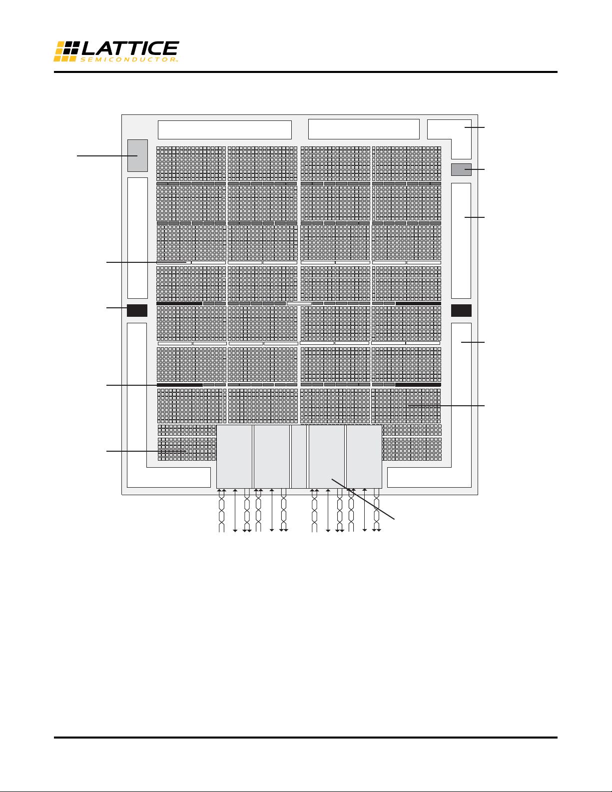
Higher Logic Density for Increased System
Integration
• Up to 35K LUTs
• 116 to 310 I/Os
Embedded SERDES
• 150 Mbps to 3.2 Gbps for Generic 8b10b, 10-bit
SERDES, and 8-bit SERDES modes
• Data Rates 230 Mbps to 3.2 Gbps per channel
for all other protocols
• Up to 4 channels per device: PCI Express,
SONET/SDH, Ethernet (1GbE, SGMII, XAUI),
CPRI, SMPTE 3G and Serial RapidIO
sysDSP™
• Fully cascadable slice architecture
• 12 to 32 slices for high performance multiply and
accumulate
• Powerful 54-bit ALU operations
• Time Division Multiplexing MAC Sharing
• Rounding and truncation
• Each slice supports
– Half 36x36, two 18x18 or four 9x9 multipliers
– Advanced 18x36 MAC and 18x18 Multiply-
Multiply-Accumulate (MMAC) operations
Flexible Memory Resources
• Up to 1.33Mbits sysMEM™ Embedded Block
RAM (EBR)
• 36K to 68K bits distributed RAM
sysCLOCK Analog PLLs and DLLs
• Two DLLs and up to four PLLs per device
Pre-Engineered Source Synchronous I/O
• DDR registers in I/O cells
• Dedicated read/write levelling functionality
• Dedicated gearing logic
• Source synchronous standards support
– ADC/DAC, 7:1 LVDS, XGMII
– High Speed ADC/DAC devices
• Dedicated DDR/DDR2/DDR3 memory with DQS
support
• Optional Inter-Symbol Interference (ISI)
correction on outputs
Programmable sysI/O™ Buffer Supports
Wide Range of Interfaces
• On-chip termination
• Optional equalization filter on inputs
• LVTTL and LVCMOS 33/25/18/15/12
• SSTL 33/25/18/15 I, II
• HSTL15 I and HSTL18 I, II
• PCI and Differential HSTL, SSTL
• LVDS, Bus-LVDS, LVPECL, RSDS, MLVDS
Flexible Device Configuration
• Dedicated bank for configuration I/Os
• SPI boot flash interface
• Dual-boot images supported
• Slave SPI
• TransFR™ I/O for simple field updates
• Soft Error Detect embedded macro
System Level Support
• IEEE 1149.1 and IEEE 1532 compliant
• Reveal Logic Analyzer
• ORCAstra FPGA configuration utility
• On-chip oscillator for initialization & general use
• 1.2V core power supply
LA-LatticeECP3 Automotive Family Data Sheet
Introduction
1-2
Introduction
LA-LatticeECP3 Automotive Family Data Sheet
Table 1-1. LA-LatticeECP3 Family Selection Guide
Introduction
The LA-LatticeECP3 automotive FPGA devices are optimized to deliver high performance features such as an
enhanced DSP architecture, high speed SERDES and high speed source synchronous interfaces in an economical
FPGA fabric. This combination is achieved through advances in device architecture and the use of 65nm technology
making the devices suitable for high-volume, high-speed, low-cost applications.
The LA-LatticeECP3 device family expands look-up-table (LUT) capacity to 35K logic elements and supports up to
310 user I/Os. The LA-LatticeECP3 device family also offers up to 64 18x18 multipliers and a wide range of parallel
I/O standards.
The LA-LatticeECP3 FPGA fabric is optimized with high performance and low cost in mind. The LA-LatticeECP3
devices utilize reconfigurable SRAM logic technology and provide popular building blocks such as LUT-based logic,
distributed and embedded memory, Phase Locked Loops (PLLs), Delay Locked Loops (DLLs), pre-engineered
source synchronous I/O support, enhanced sysDSP slices and advanced configuration support, including encryption
and dual-boot capabilities.
The pre-engineered source synchronous logic implemented in the LA-LatticeECP3 device family supports a broad
range of interface standards, including DDR3, XGMII and 7:1 LVDS.
The LA-LatticeECP3 device family also features high speed SERDES with dedicated PCS functions. High jitter toler-
ance and low transmit jitter allow the SERDES plus PCS blocks to be configured to support an array of popular data
protocols including PCI Express, SMPTE, Ethernet (XAUI, GbE, and SGMII) and CPRI. Transmit Pre-emphasis and
Receive Equalization settings make the SERDES suitable for transmission and reception over various forms of
media.
The LA-LatticeECP3 devices also provide flexible, reliable and secure configuration options, such as dual-boot capa-
bility, bitstream encryption, and TransFR field upgrade features.
The Lattice Diamond
®
design software allows large complex designs to be efficiently implemented using the LA-
LatticeECP3 FPGA family. Synthesis library support for LA-LatticeECP3 is available for popular logic synthesis tools.
Diamond tools use the synthesis tool output along with the constraints from its floor planning tools to place and route
the design in the LA-LatticeECP3 device. The tools extract the timing from the routing and back-annotate it into the
design for timing verification.
Lattice provides many pre-engineered IP (Intellectual Property) modules for the LA-LatticeECP3 family. By using
these configurable soft core IPs as standardized blocks, designers are free to concentrate on the unique aspects of
their design, increasing their productivity.
Device LA-ECP3-17 LA-ECP3-35
LUTs (K) 17 33
sysMEM Blocks (18Kbits) 38 72
Embedded Memory (Kbits) 700 1327
Distributed RAM Bits (Kbits) 36 68
18X18 Multipliers 24 64
SERDES (Quad) 1 1
PLLs/DLLs 2/2 4/2
Packages and SERDES Channels/ I/O Combinations
Package / Status LA-ECP3-17 LA-ECP3-35
328 csBGA (10x10 mm) / Advanced 2/116
256 ftBGA (17x17 mm) / Preliminary 4/133 4/133
484 fpBGA (23x23 mm) / Preliminary 4/222 4/295
672 fpBGA (27x27 mm) / Preliminary 4/310
www.latticesemi.com 2-1 DS1041 Architecture_01.0
June 2013 Advance Data Sheet DS1041
© 2013 Lattice Semiconductor Corp. All Lattice trademarks, registered trademarks, patents, and disclaimers are as listed at www.latticesemi.com/legal. All other brand
or product names are trademarks or registered trademarks of their respective holders. The specifications and information herein are subject to change without notice.
Architecture Overview
Each LA-LatticeECP3 device contains an array of logic blocks surrounded by Programmable I/O Cells (PIC). Inter-
spersed between the rows of logic blocks are rows of sysMEM™ Embedded Block RAM (EBR) and rows of sys-
DSP™ Digital Signal Processing slices, as shown in Figure 2-1. The LA-LatticeECP3 devices have two rows of
DSP slices. In addition, the LA-LatticeECP3 family contains SERDES Quads on the bottom of the device.
There are two kinds of logic blocks, the Programmable Functional Unit (PFU) and Programmable Functional Unit
without RAM (PFF). The PFU contains the building blocks for logic, arithmetic, RAM and ROM functions. The PFF
block contains building blocks for logic, arithmetic and ROM functions. Both PFU and PFF blocks are optimized for
flexibility, allowing complex designs to be implemented quickly and efficiently. Logic Blocks are arranged in a two-
dimensional array. Only one type of block is used per row.
The LA-LatticeECP3 devices contain one or more rows of sysMEM EBR blocks. sysMEM EBRs are large, dedi-
cated 18Kbit fast memory blocks. Each sysMEM block can be configured in a variety of depths and widths as RAM
or ROM. In addition, LA-LatticeECP3 devices contain up to two rows of DSP slices. Each DSP slice has multipliers
and adder/accumulators, which are the building blocks for complex signal processing capabilities.
The LA-LatticeECP3 devices feature up to 4 embedded 3.2Gbps SERDES (Serializer / Deserializer) channels.
Each SERDES channel contains independent 8b/10b encoding / decoding, polarity adjust and elastic buffer logic.
Each group of four SERDES channels, along with its Physical Coding Sub-layer (PCS) block, creates a quad. The
functionality of the SERDES/PCS quads can be controlled by memory cells set during device configuration or by
registers that are addressable during device operation. The registers in the quad can be programmed via the
SERDES Client Interface (SCI). This quad is located at the bottom of the devices.
Each PIC block encompasses two PIOs (PIO pairs) with their respective sysI/O buffers. The sysI/O buffers of the
LA-LatticeECP3 devices are arranged in seven banks, allowing the implementation of a wide variety of I/O stan-
dards. In addition, a separate I/O bank is provided for the programming interfaces. 50% of the PIO pairs on the left
and right edges of the device can be configured as LVDS transmit/receive pairs. The PIC logic also includes pre-
engineered support to aid in the implementation of high speed source synchronous standards such as XGMII, 7:1
LVDS, along with memory interfaces including DDR3.
Other blocks provided include PLLs, DLLs and configuration functions. The LA-LatticeECP3 architecture provides
two Delay Locked Loops (DLLs) and up to four Phase Locked Loops (PLLs). The PLL and DLL blocks are located
at the end of the EBR/DSP rows.
The configuration block that supports features such as configuration bit-stream decryption, transparent updates
and dual-boot support is located toward the center of this EBR row. Every device in the LA-LatticeECP3 family sup-
ports a sysCONFIG™ port located in the corner between banks one and two, which allows for serial or parallel
device configuration.
In addition, every device in the family has a JTAG port. This family also provides an on-chip oscillator and soft error
detect capability. The LA-LatticeECP3 devices use 1.2V as their core voltage.
LA-LatticeECP3 Automotive Family Data Sheet
Architecture
2-2
Architecture
LA-LatticeECP3 Automotive Family Data Sheet
Figure 2-1. Simplified Block Diagram, LA-LatticeECP3-35 Device (Top Level)
PFU Blocks
The core of the LA-LatticeECP3 device consists of PFU blocks, which are provided in two forms, the PFU and PFF.
The PFUs can be programmed to perform Logic, Arithmetic, Distributed RAM and Distributed ROM functions. PFF
blocks can be programmed to perform Logic, Arithmetic and ROM functions. Except where necessary, the remain-
der of this data sheet will use the term PFU to refer to both PFU and PFF blocks.
Each PFU block consists of four interconnected slices numbered 0-3 as shown in Figure 2-2. Each slice contains
two LUTs. All the interconnections to and from PFU blocks are from routing. There are 50 inputs and 23 outputs
associated with each PFU block.
SERDES/PCS
CH 3
SERDES/PCS
CH 2
SERDES/PCS
CH 1
SERDES/PCS
CH 0
sysIO
Bank
7
sysIO
Bank
2
sysIO
Bank 0
sysIO
Bank 1
sysIO Bank 3 sysIO Bank 6
Configuration Logic:
Dual-boot, Encryption
and Transparent Updates
On-chip Oscillator
Pre-engineered Source
Synchronous Support:
DDR3 - 800Mbps
Generic - Up to 1Gbps
Flexible Routing:
Optimized for speed
and routability
Flexible sysIO:
LVCMOS, HSTL,
SSTL, LVDS
Up to 486 I/Os
Programmable
Function Units:
Up to 149K LUTs
sysCLOCK
PLLs & DLLs:
Frequency Synthesis
and Clock Alignment
Enhanced DSP
Slices: Multiply,
Accumulate and ALU
JTAG
sysMEM Block
RAM: 18Kbit
3.2Gbps SERDES
Note: There is no Bank 4 or Bank 5 in LatticeECP3 devices.
剩余123页未读,继续阅读
资源评论
paul1001130221
- 粉丝: 0
- 资源: 4
上传资源 快速赚钱
- 我的内容管理 展开
- 我的资源 快来上传第一个资源
- 我的收益 登录查看自己的收益
- 我的积分 登录查看自己的积分
- 我的C币 登录后查看C币余额
- 我的收藏
- 我的下载
- 下载帮助
安全验证
文档复制为VIP权益,开通VIP直接复制
信息提交成功