K9F1208.pdf

K9F1208U0M-YCB0, K9F1208U0M-YIB0 FLASH MEMORY
1
Document Title
64M x 8 Bit NAND Flash Memory
Revision History
Revision No
0.0
0.1
0.2
0.3
0.4
Remark
Advanced
Information
History
1. Initial issue
1. Renamed GND input (pin # 6) on behalf of SE (pin # 6)
- The SE input controls the access of the spare area. When SE is high,
the spare area is not accessible for reading or programming. SE is rec
ommended to be coupled to GND or Vcc and should not be toggled
during reading or programming.
=> Connect this input pin to GND or set to static low state unless the
sequential read mode excluding spare area is used.
2. Updated operation for tRST timing
- If reset command(FFh) is written at Ready state, the device goes into
Busy for maximum 5us.
1. Changed GND input (pin # 6) pin to N.C ( No Connection).
- The pin # 6 is don’t-cared regardless of external logic input level
and is fixed as low internally.
1. Changed plane address in Copy-Back Program
- A24 and A25 must be the same between source and target page
=> A14 and A15 must be the same between source and target page
1. Changed DC characteristics
2. Unified access timing parameter definition for multiple operating modes
- Changed AC characteristics (Before)
- AC characteristics (After)
. Deleted tCR,tRSTO, tCSTO and tREADID / Added tCEA
Parameter Min Typ Max Unit
Operating
Current
Sequential Read - 10 20->30
mAProgram - 10 20->30
Erase - 10 20->30
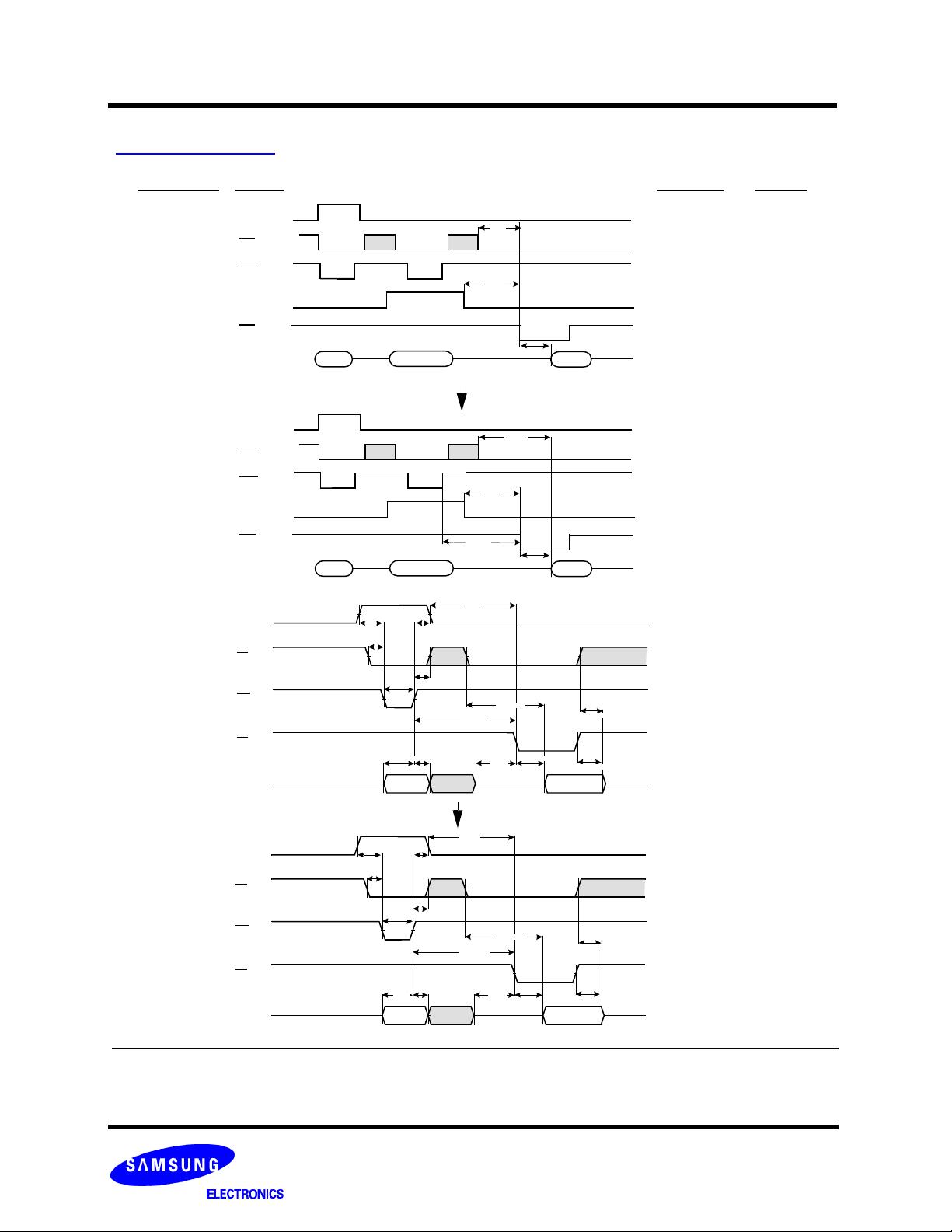
Parameter Symbol Min Max Unit
ALE to RE Delay( ID read ) tAR1 100 -
ns
CE to RE Delay( ID read) tCR 100 -
RE Low to Status Output tRSTO - 35
CE Low to Status Output tCSTO - 45
RE access time(Read ID) tREADID - 35
Parameter Symbol Min Max Unit
ALE to RE Delay( ID read ) tAR1 10 -
ns
CE Access Time tCEA - 45
Draft Date
Oct. 27th 2000
Dec. 5th 2000
Dec. 15th 2000
Jan. 8th 2001
Apr. 7th 2001
剩余40页未读,继续阅读
资源评论

 zhouli52602013-09-18用的JZ2440,数据手册
- yinababa2013-01-27用的JZ2440,数据手册下载错了。
- jingyi19812014-09-22是我想要的数据手册
- chensz7322013-04-21感谢分享,有用的datesheet
- asec43212015-10-31感谢分享,是有用的datesheet


