TDC GPX2 规格书
需积分: 38 133 浏览量
2018-12-17
14:51:03
上传
评论 1
收藏 1.36MB PDF 举报

ams Datasheet Page 1
[v1-03] 2017-Dec-18 Document Feedback
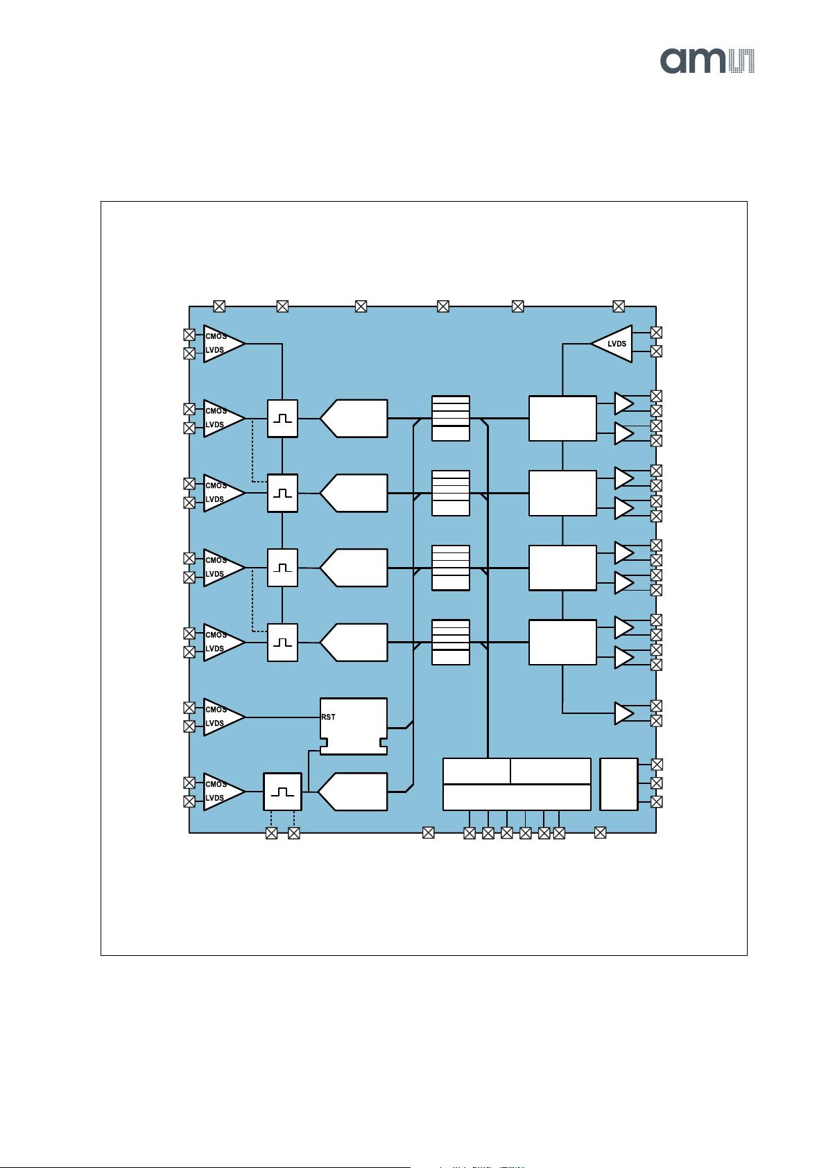
TDC-GPX2
4-Channel Time-to-Digital Converter
The GPX2 is a high performance time-to-digital converter (TDC)
frontend device.
Highest measurement performance and highest data
throughput is achieved with LVDS stop inputs and LVDS serial
outputs for each channel. Current saving operation is also
possible with CMOS inputs and SPI readout.
High configuration flexibility and unlimited measurement
range cover many applications. They range from portable
handheld laser range equipment to ambitious time-of-flight
measurements of highest performance, as e.g. done in medical
imaging applications.
GPX2 operates without any locked loop technologies. GPX2
calculates all stop measurements inside, proportional to the
applied reference clock. Combinations of best single shot
accuracy of 10ps with lowest pulse-to-pulse spacing <5ns and
maximum data throughput rate of 70MSPS per stop input are
possible.
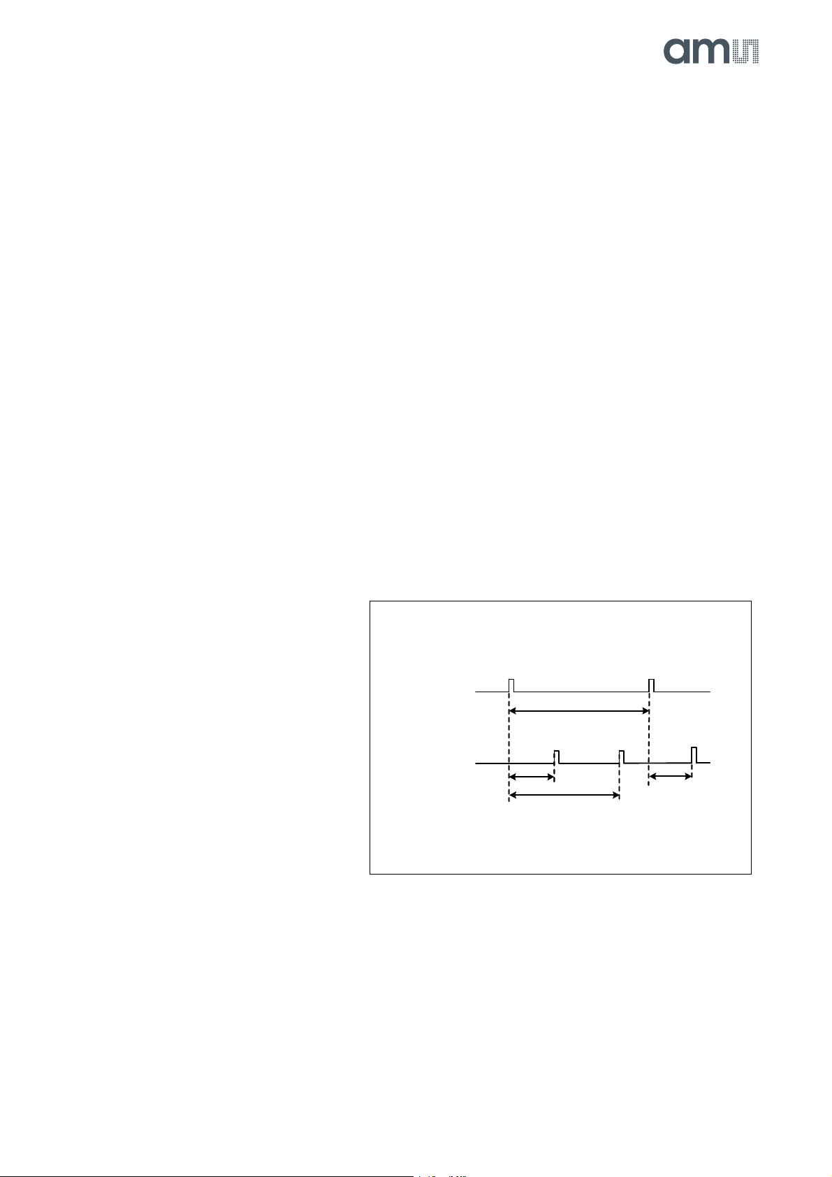
Figure 1:
Time Interval Measurements
Ordering Information and Content Guide appear at end of
datasheet.
General Description
#1
REFCLK
#2
STOP
T1
T3
T-REF
T2


剩余76页未读,继续阅读
资源评论


