


September 1990 Order Number: 231455-005
8086
16-BIT HMOS MICROPROCESSOR
8086/8086-2/8086-1
Y
Direct Addressing Capability 1 MByte
of Memory
Y
Architecture Designed for Powerful
Assembly Language and Efficient High
Level Languages
Y
14 Word, by 16-Bit Register Set with
Symmetrical Operations
Y
24 Operand Addressing Modes
Y
Bit, Byte, Word, and Block Operations
Y
8 and 16-Bit Signed and Unsigned
Arithmetic in Binary or Decimal
Including Multiply and Divide
Y
Range of Clock Rates:
5 MHz for 8086,
8 MHz for 8086-2,
10 MHz for 8086-1
Y
MULTIBUS System Compatible
Interface
Y
Available in EXPRESS
Ð Standard Temperature Range
Ð Extended Temperature Range
Y
Available in 40-Lead Cerdip and Plastic
Package
(See Packaging Spec. Order
Ý
231369)
The Intel 8086 high performance 16-bit CPU is available in three clock rates: 5, 8 and 10 MHz. The CPU is
implemented in N-Channel, depletion load, silicon gate technology (HMOS-III), and packaged in a 40-pin
CERDIP or plastic package. The 8086 operates in both single processor and multiple processor configurations
to achieve high performance levels.
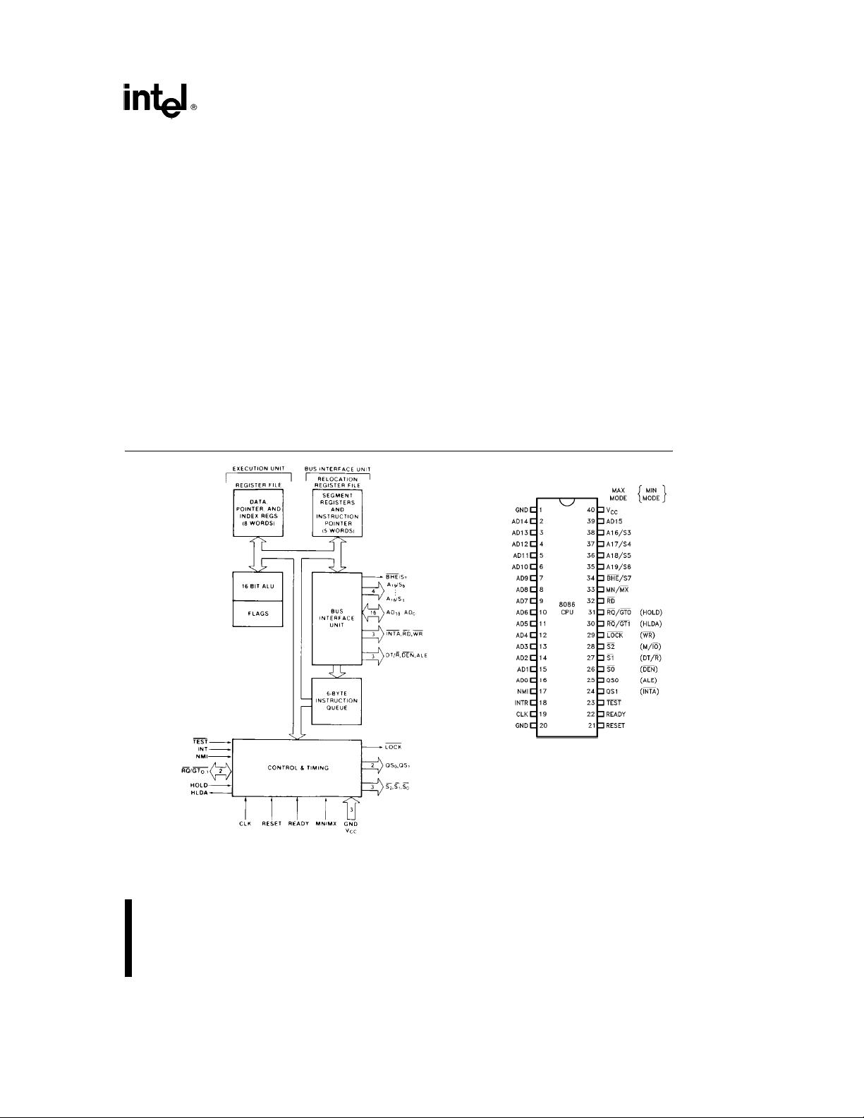
231455–1
Figure 1. 8086 CPU Block Diagram
231455–2
40 Lead
Figure 2. 8086 Pin
Configuration
8086
Table 1. Pin Description
The following pin function descriptions are for 8086 systems in either minimum or maximum mode. The ‘‘Local
Bus’’ in these descriptions is the direct multiplexed bus interface connection to the 8086 (without regard to
additional bus buffers).
Symbol Pin No. Type Name and Function
AD
15
–AD
0
2– 16, 39 I/O ADDRESS DATA BUS: These lines constitute the time multiplexed
memory/IO address (T
1
), and data (T
2
,T
3
,T
W
,T
4
) bus. A
0
is
analogous to BHE
for the lower byte of the data bus, pins D
7
–D
0
.Itis
LOW during T
1
when a byte is to be transferred on the lower portion
of the bus in memory or I/O operations. Eight-bit oriented devices tied
to the lower half would normally use A
0
to condition chip select
functions. (See BHE.) These lines are active HIGH and float to 3-state
OFF during interrupt acknowledge and local bus ‘‘hold acknowledge’’.
A
19
/S
6
, 35–38 O ADDRESS/STATUS: During T
1
these are the four most significant
address lines for memory operations. During I/O operations these
A
18
/S
5
,
lines are LOW. During memory and I/O operations, status information
A
17
/S
4
,
is available on these lines during T
2
,T
3
,T
W
,T
4
. The status of the
A
16
/S
3
interrupt enable FLAG bit (S
5
) is updated at the beginning of each
CLK cycle. A
17
/S
4
and A
16
/S
3
are encoded as shown.
This information indicates which relocation register is presently being
used for data accessing.
These lines float to 3-state OFF during local bus ‘‘hold acknowledge.’’
A
17
/S
4
A
16
/S
3
Characteristics
0 (LOW) 0 Alternate Data
0 1 Stack
1 (HIGH) 0 Code or None
1 1 Data
S
6
is 0
(LOW)
BHE/S
7
34 O BUS HIGH ENABLE/STATUS: During T
1
the bus high enable signal
(BHE
) should be used to enable data onto the most significant half of
the data bus, pins D
15
–D
8
. Eight-bit oriented devices tied to the upper
half of the bus would normally use BHE to condition chip select
functions. BHE
is LOW during T
1
for read, write, and interrupt
acknowledge cycles when a byte is to be transferred on the high
portion of the bus. The S
7
status information is available during T
2
,
T
3
, and T
4
. The signal is active LOW, and floats to 3-state OFF in
‘‘hold’’. It is LOW during T
1
for the first interrupt acknowledge cycle.
BHE A
0
Characteristics
0 0 Whole word
0 1 Upper byte from/to odd address
1 0 Lower byte from/to even address
1 1 None
RD 32 O READ: Read strobe indicates that the processor is performing a
memory or I/O read cycle, depending on the state of the S
2
pin. This
signal is used to read devices which reside on the 8086 local bus. RD
is active LOW during T
2
,T
3
and T
W
of any read cycle, and is
guaranteed to remain HIGH in T
2
until the 8086 local bus has floated.
This signal floats to 3-state OFF in ‘‘hold acknowledge’’.
2
8086
Table 1. Pin Description (Continued)
Symbol Pin No. Type Name and Function
READY 22 I READY: is the acknowledgement from the addressed memory or I/O
device that it will complete the data transfer. The READY signal from
memory/IO is synchronized by the 8284A Clock Generator to form
READY. This signal is active HIGH. The 8086 READY input is not
synchronized. Correct operation is not guaranteed if the setup and hold
times are not met.
INTR 18 I INTERRUPT REQUEST: is a level triggered input which is sampled
during the last clock cycle of each instruction to determine if the
processor should enter into an interrupt acknowledge operation. A
subroutine is vectored to via an interrupt vector lookup table located in
system memory. It can be internally masked by software resetting the
interrupt enable bit. INTR is internally synchronized. This signal is
active HIGH.
TEST 23 I TEST: input is examined by the ‘‘Wait’’ instruction. If the TEST input is
LOW execution continues, otherwise the processor waits in an ‘‘Idle’’
state. This input is synchronized internally during each clock cycle on
the leading edge of CLK.
NMI 17 I NON-MASKABLE INTERRUPT: an edge triggered input which causes
a type 2 interrupt. A subroutine is vectored to via an interrupt vector
lookup table located in system memory. NMI is not maskable internally
by software. A transition from LOW to HIGH initiates the interrupt at the
end of the current instruction. This input is internally synchronized.
RESET 21 I RESET: causes the processor to immediately terminate its present
activity. The signal must be active HIGH for at least four clock cycles. It
restarts execution, as described in the Instruction Set description, when
RESET returns LOW. RESET is internally synchronized.
CLK 19 I CLOCK: provides the basic timing for the processor and bus controller.
It is asymmetric with a 33% duty cycle to provide optimized internal
timing.
V
CC
40 V
CC
:
a
5V power supply pin.
GND 1, 20 GROUND
MN/MX 33 I MINIMUM/MAXIMUM: indicates what mode the processor is to
operate in. The two modes are discussed in the following sections.
The following pin function descriptions are for the 8086/8288 system in maximum mode (i.e., MN/MX
e
V
SS
).
Only the pin functions which are unique to maximum mode are described; all other pin functions are as
described above.
S
2
,S
1
,S
0
26–28 O STATUS: active during T
4
,T
1
, and T
2
and is returned to the passive state
(1, 1, 1) during T
3
or during T
W
when READY is HIGH. This status is used
by the 8288 Bus Controller to generate all memory and I/O access control
signals. Any change by S
2
,S
1
,orS
0
during T
4
is used to indicate the
beginning of a bus cycle, and the return to the passive state in T
3
or T
W
is
used to indicate the end of a bus cycle.
3
8086
Table 1. Pin Description (Continued)
Symbol Pin No. Type Name and Function
S
2
,S
1
,S
0
26– 28 O These signals float to 3-state OFF in ‘‘hold acknowledge’’. These status
lines are encoded as shown.
(Continued)
S
2
S
1
S
0
Characteristics
0 (LOW) 0 0 Interrupt Acknowledge
0 0 1 Read I/O Port
0 1 0 Write I/O Port
0 1 1 Halt
1 (HIGH) 0 0 Code Access
1 0 1 Read Memory
1 1 0 Write Memory
1 1 1 Passive
RQ/GT
0
, 30, 31 I/O REQUEST/GRANT: pins are used by other local bus masters to force
the processor to release the local bus at the end of the processor’s
RQ
/GT
1
current bus cycle. Each pin is bidirectional with RQ/GT
0
having higher
priority than RQ
/GT
1
.RQ/GT pins have internal pull-up resistors and
may be left unconnected. The request/grant sequence is as follows
(see Page 2-24):
1. A pulse of 1 CLK wide from another local bus master indicates a local
bus request (‘‘hold’’) to the 8086 (pulse 1).
2. During a T
4
or T
1
clock cycle, a pulse 1 CLK wide from the 8086 to
the requesting master (pulse 2), indicates that the 8086 has allowed the
local bus to float and that it will enter the ‘‘hold acknowledge’’ state at
the next CLK. The CPU’s bus interface unit is disconnected logically
from the local bus during ‘‘hold acknowledge’’.
3. A pulse 1 CLK wide from the requesting master indicates to the 8086
(pulse 3) that the ‘‘hold’’ request is about to end and that the 8086 can
reclaim the local bus at the next CLK.
Each master-master exchange of the local bus is a sequence of 3
pulses. There must be one dead CLK cycle after each bus exchange.
Pulses are active LOW.
If the request is made while the CPU is performing a memory cycle, it
will release the local bus during T
4
of the cycle when all the following
conditions are met:
1. Request occurs on or before T
2
.
2. Current cycle is not the low byte of a word (on an odd address).
3. Current cycle is not the first acknowledge of an interrupt acknowledge
sequence.
4. A locked instruction is not currently executing.
If the local bus is idle when the request is made the two possible events
will follow:
1. Local bus will be released during the next clock.
2. A memory cycle will start within 3 clocks. Now the four rules for a
currently active memory cycle apply with condition number 1 already
satisfied.
LOCK 29 O LOCK: output indicates that other system bus masters are not to gain
control of the system bus while LOCK
is active LOW. The LOCK signal
is activated by the ‘‘LOCK’’ prefix instruction and remains active until the
completion of the next instruction. This signal is active LOW, and floats
to 3-state OFF in ‘‘hold acknowledge’’.
4
8086
Table 1. Pin Description (Continued)
Symbol Pin No. Type Name and Function
QS
1
,QS
0
24, 25 O QUEUE STATUS: The queue status is valid during the CLK cycle after
which the queue operation is performed.
QS
1
and QS
0
provide status to allow external tracking of the internal
8086 instruction queue.
QS
1
QS
0
Characteristics
0 (LOW) 0 No Operation
0 1 First Byte of Op Code from Queue
1 (HIGH) 0 Empty the Queue
1 1 Subsequent Byte from Queue
The following pin function descriptions are for the 8086 in minimum mode (i.e., MN/MX
e
V
CC
). Only the pin
functions which are unique to minimum mode are described; all other pin functions are as described above.
M/IO 28 O STATUS LINE: logically equivalent to S
2
in the maximum mode. It is used to
distinguish a memory access from an I/O access. M/IO
becomes valid in
the T
4
preceding a bus cycle and remains valid until the final T
4
of the cycle
(M
e
HIGH, IO
e
LOW). M/IO floats to 3-state OFF in local bus ‘‘hold
acknowledge’’.
WR 29 O WRITE: indicates that the processor is performing a write memory or write
I/O cycle, depending on the state of the M/IO
signal. WR is active for T
2
,T
3
and T
W
of any write cycle. It is active LOW, and floats to 3-state OFF in
local bus ‘‘hold acknowledge’’.
INTA 24 O INTA: is used as a read strobe for interrupt acknowledge cycles. It is active
LOW during T
2
,T
3
and T
W
of each interrupt acknowledge cycle.
ALE 25 O ADDRESS LATCH ENABLE: provided by the processor to latch the
address into the 8282/8283 address latch. It is a HIGH pulse active during
T
1
of any bus cycle. Note that ALE is never floated.
DT/R 27 O DATA TRANSMIT/RECEIVE: needed in minimum system that desires to
use an 8286/8287 data bus transceiver. It is used to control the direction of
data flow through the transceiver. Logically DT/R
is equivalent to S
1
in the
maximum mode, and its timing is the same as for M/IO
.(T
e
HIGH, R
e
LOW.) This signal floats to 3-state OFF in local bus ‘‘hold acknowledge’’.
DEN 26 O DATA ENABLE: provided as an output enable for the 8286/8287 in a
minimum system which uses the transceiver. DEN is active LOW during
each memory and I/O access and for INTA cycles. For a read or INTA
cycle
it is active from the middle of T
2
until the middle of T
4
, while for a write cycle
it is active from the beginning of T
2
until the middle of T
4
. DEN floats to 3-
state OFF in local bus ‘‘hold acknowledge’’.
HOLD, 31, 30 I/O HOLD: indicates that another master is requesting a local bus ‘‘hold.’’ To be
acknowledged, HOLD must be active HIGH. The processor receiving the
HLDA
‘‘hold’’ request will issue HLDA (HIGH) as an acknowledgement in the
middle of a T
4
or T
i
clock cycle. Simultaneous with the issuance of HLDA
the processor will float the local bus and control lines. After HOLD is
detected as being LOW, the processor will LOWer the HLDA, and when the
processor needs to run another cycle, it will again drive the local bus and
control lines. Hold acknowledge (HLDA) and HOLD have internal pull-up
resistors.
The same rules as for RQ
/GT apply regarding when the local bus will be
released.
HOLD is not an asynchronous input. External synchronization should be
provided if the system cannot otherwise guarantee the setup time.
5


