没有合适的资源?快使用搜索试试~ 我知道了~
CXA1145 Datasheet
需积分: 20 0 下载量 82 浏览量
2020-11-28
11:51:55
上传
评论
收藏 362KB PDF 举报
温馨提示
试读
15页
The CXA 1145P/M encoder converts an ana- log.RGB signal to a composite video signal. CXA 1145P 24 pin DIP With its built-in circuit various pulses required for an encoder, composite video outputs are ob- tained just by inputting the composite sync and analog RGB signal.
资源详情
资源评论
资源推荐
II
8382383
0005301
056
IISONV
SONY
.
CXA
1145P/M
RGB Encoder
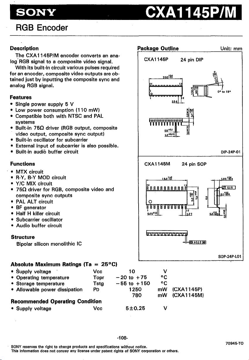
Description Packa e Outline Unit: mm
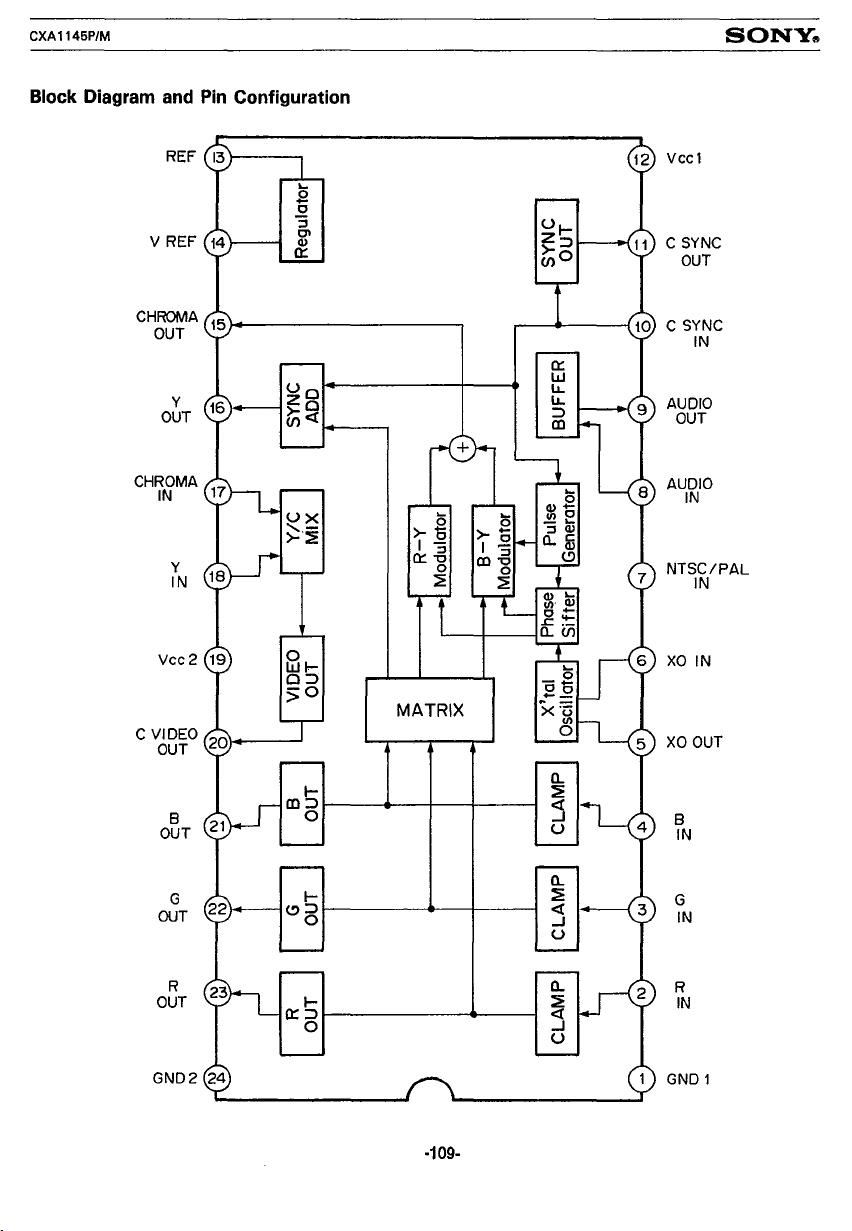
The
CXA 1145P/M encoder converts
an
ana-
log.RGB signal
to
a composite video signal.
CXA 1145P 24
pin
DIP
With its built-in circuit various pulses required
for
an
encoder, composite video outputs
are
ob-
tained just by inputting the composite sync and
analog
RGB
signal.
Features
• Single power supply 5 V
•
Low power consumption (
11
0 mWI
• Compatible
both
with
NTSC and PAL
systems
• Built-in
750
driver
(RGB
output, composite
video output, composite sync output)
• Built-in oscillator for subcarrier
• External input
of
subcarrier is also possible.
• Built-in audio buffer circuit
Functions
CXA1145M
24
pin
SOP
• MTX circuit
•
R-Y,
B-Y MOD circuit
• Y/C MIX circuit
"
•
750
driver
for
RGB,
composite video and
composite sync outputs
• PAL AL T circuit
•
BF
generator
• Half H killer circuit
• Subcarrier oscillator
•
Audio buffer circuit
Structure
Bipolar silicon monolithic
IC
Absolute Maximum Ratings (Ta =
25°C)
• Supply voltage · Vee
• Operating temperature Topr
• Storage temperature Tstg
• Allowable power dissipation
Po
Recommended Operating Condition
• Supply voltage Vee
10
-20
to
+75
-55
to
+
150
1250
780
5±0.25
-108-
SONY
reserves the right
to
change products and specifications
without
notice.
v
oc
oc
mW
(CXA 1145P)
mW (CXA
1145MI
v
This Information does not convey any license under patent rights
of
SONY corporation or others.
DIP-24P-01
SOP·24P-L01
70945-TO
..
8382383
0005302
T92
..
SONY
CXA1145P/M
SONY
..
Block Diagram and Pin Configuration
C
SYNC
OUT
CHROMA
C
SYNC
OUT
IN
y
AUDIO
OUT
OUT
CHROMA
AUDIO
I
IN
IN
y
NTSC/PAL
IN
IN
C
VIDEO
OUT
B
B
OUT
IN
G
G
OUT
IN
R
R
OUT
IN
·109-
..
8382383
0005303
929
..
SONY
CXA1146P/M
SONY.,
Pin
Description
No.
Symbol Equivalent circuit
Description
GND
pin for circuits other than
o~tputs
of
RGB
1
GND
1
and
composite video.
Connect with
GND
2 using
an
impedance
as
low
as
possible.
k
'
)-
,___
2
RIN
l
Input pin for the analog
RGB
signal.
3
GIN
2
Input with 100% = 1 Vp-p.
It
is necessary to
4
BIN
~
input with
an
impedance
as
low
as
possible to
®
+
minimize the clamp error allowance.
@)
r/r
6
XO
OUT
5
t
Ji'>r
Pin
for the x'tal
OSC.
For
inner oscillation. a crystal oscillator is con·
nected.
For
external oscillation, Input
to
pin 6
XO
IN
through a coupling capacitor.
Input with the sub-carrier Input level at
400
mVp-p to 1,000 mVp-p.
For
external oscillation, input a
sine
wave with
enough
less
distortion. With much distortion,
1
the chroma signal's
phase
property may de·
teriorate.
6
XOIN
6
+
+
"
.
j
J
J
Switching pin between
NTSC
and
PAL
mode.
7
NTSC/PAL
.
Vee
NTSC
IN
7 I
I
I
GND
PAL
,...,.
·110-
剩余14页未读,继续阅读
jccha
- 粉丝: 0
- 资源: 4
上传资源 快速赚钱
- 我的内容管理 展开
- 我的资源 快来上传第一个资源
- 我的收益 登录查看自己的收益
- 我的积分 登录查看自己的积分
- 我的C币 登录后查看C币余额
- 我的收藏
- 我的下载
- 下载帮助
安全验证
文档复制为VIP权益,开通VIP直接复制
信息提交成功
评论0