没有合适的资源?快使用搜索试试~ 我知道了~
ISSI DDR2 128Mx16 data sheet
需积分: 0 8 下载量 3 浏览量
2011-05-11
00:22:41
上传
评论 1
收藏 446KB PDF 举报
温馨提示
试读
26页
2Gb (x16) DDR2 SDRAM
资源详情
资源评论
资源推荐
IS43/46DR16128
Integrated Silicon Solution, Inc. – www.issi.com – 1
Rev. 00B, 3/28/2011
2Gb (x16) DDR2 SDRAM
FEATURES
Clockfrequencyupto400MHz
8internalbanksforconcurrentoperation
4‐bitprefetcharchitecture
ProgrammableCASLatency:3,4,5,6and7
ProgrammableAdditiveLatency:0,1,2,3,4,5
and6
WriteLatency=ReadLatency‐1
ProgrammableBurstSequence:
Sequentialor
Interleave
ProgrammableBurstLength:4and8
AutomaticandControlledPrechargeCommand
PowerDownMode
AutoRefreshandSelfRefresh
RefreshInterval:7.8s(8192cycles/64ms)
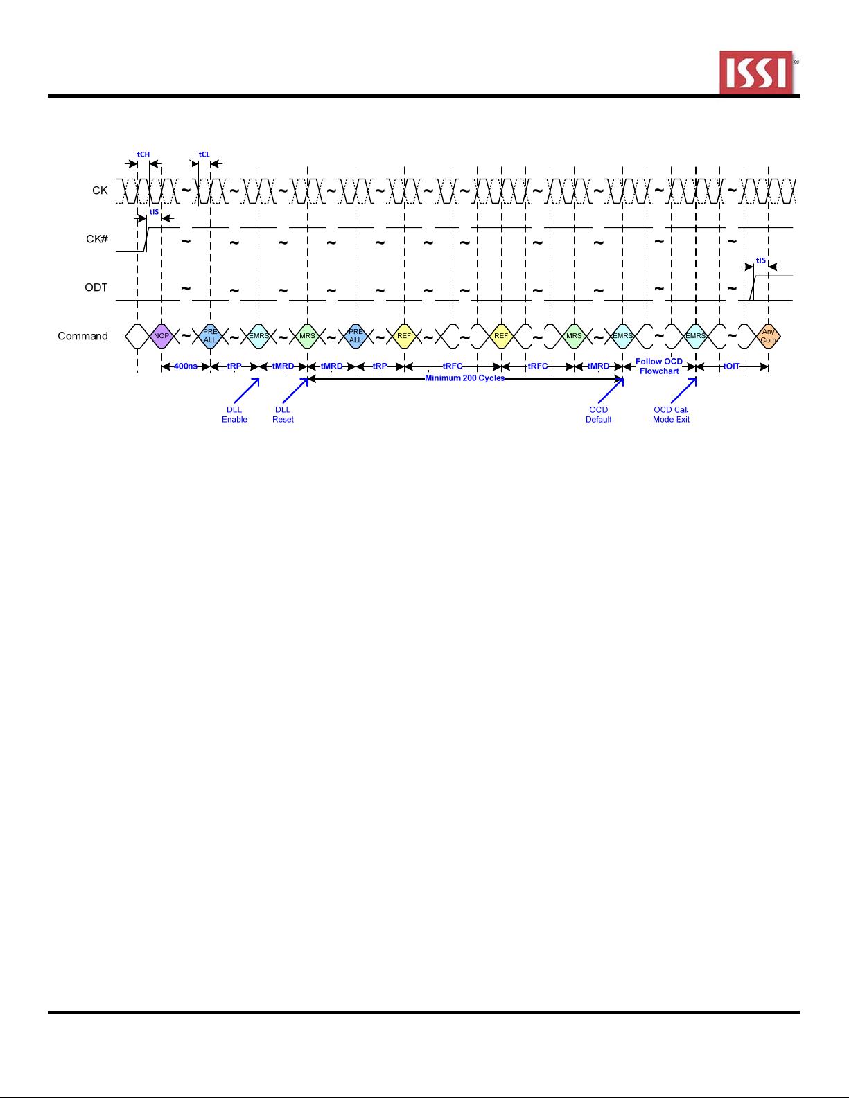
OCD(Off‐ChipDriverImpedanceAdjustment)
ODT(On‐DieTermination)
WeakStrengthData
‐OutputDriverOption
BidirectionaldifferentialDataStrobe(Single‐
endeddata‐strobeisanoptionalfeature)
On‐ChipDLLalignsDQandDQstransitionswith
CKtransitions
DQS#canbedisabledforsingle‐endeddata
strobe
DifferentialclockinputsCKandCK#
VDDandVDDQ=
1.8V±0.1V
PASR(PartialArraySelfRefresh)
SSTL_18interface
tRASlockoutsupported
Operatingtemperature:
Commercial(T
A
=0°Cto70°C;T
C
=0°Cto85°C)
Industrial(T
A
=‐40°Cto85°C;T
C
=‐40°Cto95°C)
2
Automotive,A1(T
A
=‐40°Cto85°C;T
C
=‐40°Cto95°C)
2
Automotive,A2(T
A
=‐40°Cto105°C;T
C
=‐40°Cto
105°C)
2
OPTIONS
Configuration:
128Mx16(twostacked16 Mx8x8banks)
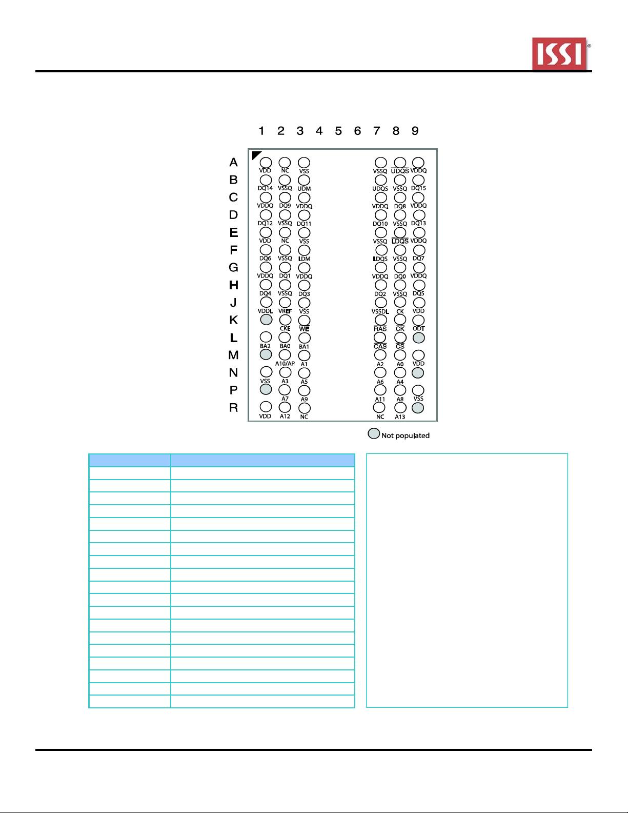
Package:
84‐ballFBGA
ADDRESSTABLE
Parameter 128Mx16
RowAddressing A0‐A13
ColumnAddressing A0‐A9
BankAddressing BA0‐BA2
PrechargeAddressing A10
ClockCycleTiming
‐37C ‐3D ‐25E ‐25D Units
SpeedGrade DDR2‐533C DDR2‐667D DDR2‐800E DDR2‐800D
CL‐tRCD‐tRP 4‐4‐4 5‐5‐5 6‐6‐6 5‐5‐5 tCK
tCK(CL=3) 5 5 5 5 ns
tCK(CL=4) 3.75 3.75 3.75 3.75 ns
tCK(CL=5) 3.75 3 3 2.5 ns
tCK(CL=6) 3.75 3 2.5 2.5 ns
tCK(CL=7) 3.75 3 2.5 2.5 ns
Frequency(max) 266 333 400 400 MHz
Note:
1. The‐37C,‐25Eand‐25Ddevicespecificationsareshownforreferenceonly.
2. PleasecontactISSIforavailabilityofAutomotiveparts.
PRELIMINARYINFORMATION
APRIL2011
Copyright © 2011 Integrated Silicon Solution, Inc. All rights reserved. ISSI reserves the right to make changes to this specification and its products at any time
without notice. ISSI assumes no liability arising out of the application or use of any information, products or services described herein. Customers are advised to
obtain the latest version of this device specification before relying on any published information and before placing orders for products.
Integrated Silicon Solution, Inc. does not recommend the use of any of its products in life support applications where the failure or malfunction of the product can
reasonably be expected to cause failure of the life support system or to significantly affect its safety or effectiveness. Products are not authorized for use in such
applications unless Integrated Silicon Solution, Inc. receives written assurance to its satisfaction, that:
a.) the risk of injury or damage has been minimized;
b.) the user assume all such risks; and
c.) potential liability of Integrated Silicon Solution, Inc is adequately protected under the circumstances
IS43/46DR16128
Integrated Silicon Solution, Inc. – www.issi.com – 2
Rev. 00B, 3/28/2011
DDR2SDRAM(64Mx16)BGABall‐out(Top‐View)(10.5mmx13.5mmBody,0.8mmpitch)
Description
Inputclocks
Clockenable
ChipSelect
Commandcontrolinputs
Address
BankAddress
I/O
UpperByteDataStrobe
LowerByteDataStrobe
Inputdatamask
Supplyvoltage
Ground
DQpowersupply
DQground
Referencevoltage
DLLpowersupply
DLLground
OnDieTerminationEnable
Noconnect
Symbol
CK,CK#
CKE
CS#
DQ[15:0]
UDQS,UDQS#
LDQS,LDQS#
UDM,LDM
RAS#,CAS#,WE#
A[13:0]
BA[2:0]
VREF
VDDL
VSSDL
NC
ODT
VDD
VSS
VDDQ
VSSQ
Note:
VDDLandVSSDLarepowerandgroundfortheDLL.Itis
recommendedthattheyareisolatedonthedevicefrom
VDD,VDDQ,VSS,andVSSQ.
IS43/46DR16128
Integrated Silicon Solution, Inc. – www.issi.com – 3
Rev. 00B, 3/28/2011
FunctionalDescription
Power‐upandInitialization
DDR2SDRAMsmustbepoweredupandinitializedinapredefinedmanner.Operationalproceduresotherthanthosespecifiedmay
resultinundefinedoperation.
Power‐upandInitializationSequence
ThefollowingsequenceisrequiredforPower‐upandInitialization.
1. EitheroneofthefollowingsequenceisrequiredforPower‐up:
A. Whileapplyingpower, attempttomaintain CKEbelow0.2 xVDDQandODT
1
at aLOWstate (allotherinputsmay be
undefined.) The VDD voltage ramp time must be no greater than 200 ms from when VDD ramps from 300 mV to
VDD(Min); and during the VDD voltage ramp, |VDD‐VDDQ|≥0.3 V. Once the ramping of the supply voltages is
complete
(whenVDDQcrossesVDDQ(Min)),thesupplyvoltagespecificationsprovidedinthetableRecommendedDC
OperatingConditions(SSTL_1.8),prevail.
VDD,VDDLandVDDQaredrivenfromasinglepowerconverteroutput,AND
VTTislimitedto0.95Vmax,AND
VREFtracksVDDQ/2,VREFmustbewithin±300mV
withrespecttoVDDQ/2duringsupplyramptime.
VDDQ≥VREFmustbemetatalltimes
B. Whileapplyingpower, attempttomaintain CKEbelow0.2 xVDDQandODT
1
at aLOWstate (allotherinputsmay be
undefined,voltagelevelsatI/OsandoutputsmustbelessthanVDDQduringvoltageramptimetoavoidDRAMlatch‐
up.Duringtherampingofthe supplyvoltages,VDD≥VDDL≥VDDQmustbemaintainedandisapplicabletobothAC
and
DClevelsuntiltherampingofthesupplyvoltagesiscomplete,whichiswhenVDDQcrossesVDDQmin.Oncethe
rampingof thesupplyvoltages iscomplete,thesupply voltagespecificationsprovided inthe tableRecommendedDC
OperatingConditions(SSTL‐1.8),prevail.
ApplyVDD/VDDLbeforeoratthesame
timeasVDDQ.
VDD/VDDLvoltageramptimemustbenogreater200msfromwhenVDDrampsfrom300mVtoVDD(Min).
ApplyVDDQbeforeoratthesametimeasVTT.
TheVDDQ voltage ramp time from when VDD(Min) is achieved on VDD to the VDDQ(Min)
is achieved on VDDQ
mustbenogreaterthan500ms.
2. Startclockandmaintainstablecondition.
3. Fortheminimumof200µsafterstablepower(VDD,VDDL,VDDQ,VREF,andVTTvaluesareintherangeoftheminimumand
maximumvaluesspecifiedinthetableRecommended
DCOperatingConditions(SSTL‐1.8))andstableclock(CK,CK#),thenapply
NOPorDeselectandassertalogicHIGHtoCKE.
4. Waitminimumof400nsthenissueaprechargeallcommand.Duringthe400nsperiod,aNOPorDeselectcommandmustbe
issuedtotheDRAM.
5.
IssueanEMRScommandtoEMR(2).
6. IssueanEMRScommandtoEMR(3).
7. IssueEMRStoenableDLL.
8. IssueaModeRegisterSetcommandforDLLreset.
9. Issueaprechargeallcommand.
10. Issue2ormoreauto‐refreshcommands.
11. IssueaMRScommandwithLOW
toA8toinitializedeviceoperation.(i.e.toprogramoperatingparameterswithoutresetting
theDLL.)
12. Waitatleast200clockcyclesafterstep8andthenexecuteOCDCalibration(OffChipDriverimpedanceadjustment).IfOCD
calibrationisnotused,EMRSDefaultcommand(A9=A8=A7=HIGH)followedbyEMRSOCDCalibrationMode
Exitcommand
(A9=A8=A7=LOW)mustbeissuedwithotheroperatingparametersofEMR(1).
13. TheDDR2SDRAMisnowreadyfornormaloperation.
Note:
1. ToguaranteeODToff,VREFmustbevalidandaLOWlevelmustbeappliedtotheODTpin.
IS43/46DR16128
Integrated Silicon Solution, Inc. – www.issi.com – 4
Rev. 00B, 3/28/2011
InitializationSequenceafterPower‐UpDiagram
ProgrammingtheModeRegisterandExtendedModeRegisters
For application flexibility, burst length, burst type, CAS# latency, DLL reset function, write recovery time (WR) are user defined
variablesandmustbeprogrammedwithaModeRegisterSet(MRS)command.Additionally,DLLdisablefunction,driverimpedance,
additiveCASlatency,ODT(OnDieTermination),single‐endedstrobe,andOCD(offchip
driverimpedanceadjustment)arealsouser
definedvariablesandmustbeprogrammedwithanExtendedModeRegisterSet(EMRS)command.ContentsoftheModeRegister
(MR)orExtendedModeRegistersEMR[1]andEMR[2]canbealteredbyre‐executingtheMRSorEMRSCommands.Eveniftheuser
chooses to
modify only a subset of the MR, EMR[1], or EMR[2] variables, all variables within the addressed register must be
redefinedwhentheMRSorEMRScommandsareissued.
MRS,EMRSandResetDLLdonotaffectmemoryarraycontents,whichmeanre‐initializationincludingthosecanbeexecutedatany
timeafterpower‐upwithoutaffectingmemoryarraycontents.
DDR2ModeRegister(MR)Setting
The mode register stores the data for controlling the various operating modes of DDR2 SDRAM. It controls CAS# latency, burst
length,burstsequence,DLLreset,tWRandactivepowerdownexittimetomakeDDR2SDRAMusefulforvariousapplications.The
defaultvalueofthemoderegisterisnotdefined,therefore
themoderegistermustbewrittenafterpower‐upforproperoperation.
Themoderegisteriswrittenby assertingLOWonCS#,RAS#,CAS#,WE#,BA0,BA1,and BA2whilecontrollingthestateofaddress
pinsA0‐A13.TheDDR2SDRAMshouldbeinallbankprechargewithCKEalready
HIGHpriortowritingintothemoderegister.The
moderegistersetcommandcycletime(tMRD)isrequiredtocompletethewriteoperationtothemoderegister.Themoderegister
contentscanbechangedusingthesamecommandandclockcyclerequirementsduringnormaloperationaslongasallbanksare
in
theprechargestate.The moderegister isdivided intovarious fieldsdependingon functionality.Burstlength isdefinedbyA0‐A2
withoptionsof4and8bitburstlengths.TheburstlengthdecodesarecompatiblewithDDRSDRAM.Burstaddresssequencetypeis
definedbyA3;CASlatency
isdefinedbyA4‐A6.TheDDR2doesn’tsupporthalfclocklatencymode.A7isusedfortestmode.A8is
usedforDLLreset.A7mustbesettoLOWfornormalMRSoperation.WriterecoverytimetWRisdefinedbyA9‐A11.Refertothe
tableforspecificcodes.
IS43/46DR16128
Integrated Silicon Solution, Inc. – www.issi.com – 5
Rev. 00B, 3/28/2011
ModeRegister(MR)Diagram
A12
0
BA2
0
1
BA1
0
BA0
0
A11 A10 A9
A13
0
000
001
010
011
100
101
110
111
A8
0A7
10
1
A6 A5 A4
000
001
010
011
100
101
110
111
A3
0
1
A2 A1 A0 BL
0104
0118
5
WR
(
c
y
cles
)
(1)
Slowexit(usetXARDS)
Activepowerdownexittime
Fastexit(usetXARD)
Normal
7
A9
8
Reserved
A12 PD1
2
3
4
4
A10
6
Yes
Reserved
A8 DLL
DLLReset
ModeNo
CASLatency
Reserved
A5
Reserved
Reserved
A4
3
Interleave
A3 BT
5
6
7
A1
BurstType
Sequential
A0
Address
Field
Mode
Register
A2
Burst
Length
A6
CAS
Latency
A7 TM
A11
WR
Notes:
1. WR(writerecoveryforautoprecharge)minisdeterminedbytCKmaxandWRmaxisdeterminedbytCKmin.WRinclockcyclesiscal culatedbydividingtWR(in
ns)bytCK(inns)androundingupanon‐integervaluetothenextinteger(WR[cycles]=tWR(ns)/tCK(ns)).Themode
registermustbeprogrammedtothisvalue.
ThisisalsousedwithtRPtodeterminetDAL.
DDR2ExtendedModeRegister1(EMR[1])Setting
The extended mode register 1 stores the data for enabling or disabling the DLL, output driver strength, ODT value selection and
additive latency. The default value of the extended mode register is not defined, therefore the extended mode register must be
writtenafterpower‐upforproperoperation.Extendedmoderegister
1iswrittenbyassertingLOWonCS#,RAS#,CAS#,WE#,BA1,
andBA2,andHIGHonBA0,andcontrollingpinsA0–A13.TheDDR2SDRAMshouldbeinallbankprechargewithCKEalreadyHIGH
priortowritingintotheextendedmoderegister.Themoderegistersetcommand
cycletime(tMRD)mustbesatisfiedtocomplete
the write operation to the extended mode register. Mode register contents can be changed using the same command and clock
cyclerequirementsduringnormaloperationaslongasallbanksareintheprechargestate.A0isusedforDLLenableordisable.
A1is
usedforenablingreducedstrengthdata‐outputdriver.A3‐A5determinestheadditivelatency,A2andA6areusedforODTvalue
selection,A7‐A9areusedforOCDcontrol,A10isusedforDQS#disableandA11isusedforRDQSenable.
剩余25页未读,继续阅读
fingandy
- 粉丝: 0
- 资源: 2
上传资源 快速赚钱
- 我的内容管理 展开
- 我的资源 快来上传第一个资源
- 我的收益 登录查看自己的收益
- 我的积分 登录查看自己的积分
- 我的C币 登录后查看C币余额
- 我的收藏
- 我的下载
- 下载帮助
安全验证
文档复制为VIP权益,开通VIP直接复制
信息提交成功
评论0