没有合适的资源?快使用搜索试试~ 我知道了~
DLP 6401 投影必备
需积分: 10 11 下载量 39 浏览量
2015-08-03
15:41:59
上传
评论
收藏 2.16MB PDF 举报
温馨提示
试读
67页
0.45dlp光机 必备 开发720p投影必须的投影芯片。 目前最成熟的应用
资源推荐
资源详情
资源评论
REVISIONS
REV DESCRIPTION TIS DOC # DATE APPROVED
0.1 Early preliminary Release N/A 06/07/2010
A Initial Release – ECR # 2110632 09/30/2010 WJS
TEXAS INSTRUMENTS
INCORPORATED
(c) COPYRIGHT 2010 TEXAS INSTRUMENTS
UNPUBLISHED, ALL RIGHTS RESERVED
DWN/CHK
Bill Sexton
DATE
09/01/10
ASIC Specification
ENGR
Jeff Kordel
DATE
09/01/10
Data Sheet,
314AS
MANU
Don Wu
DATE
09/27/10
DPP6401
NHA
USED ON
QA
Richard Gall
DATE
09/27/10
SIZE
A
2511278
APPLICATION
APVD
Don Holamon
DATE
09/28/10
SCALE
NONE
SHEET 1 OF 67
TI Confidential
NDA Restrictions
** DPP6401 **
DLP
®
PICO™PROCESSOR 6401 ASIC,
DATA SHEET
TI Confidential
NDA Restrictions
DPP6401
DLP
®
DATA PROCESSOR
DLPS011 – SEPTEMBER 2010
TI CONFIDENTIAL
NDA RESTRICTIONS
•
−
−
−
•
−
−
•
•
•
•
•
−
−
−
−
−
−
−
−
−
•
−
−
−
−
−
−
−
−
−
−
−
•
•
−
−
•
•
−
−
•
−
−
•
•
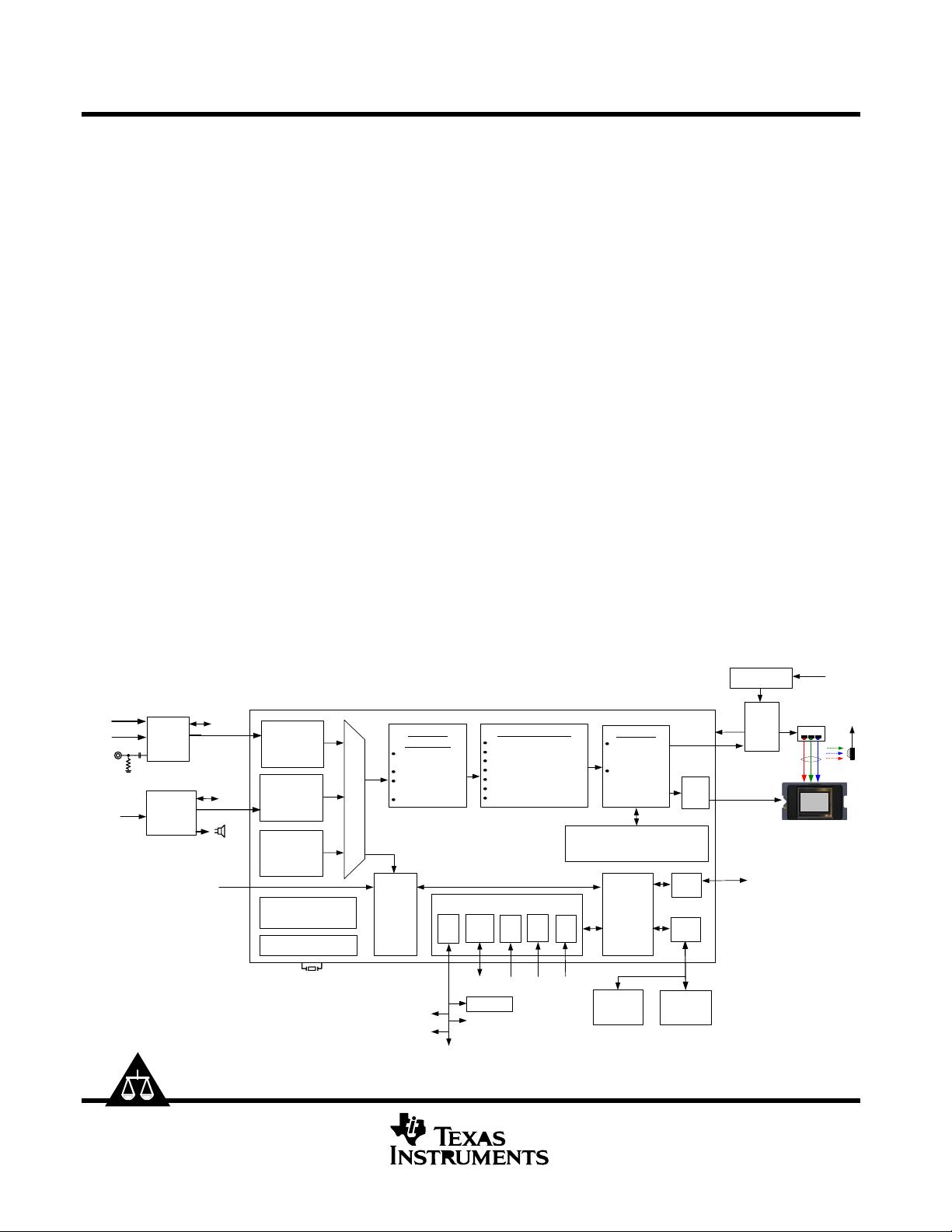
Provides a 30-bit Input Pixel Interface:
YUV, YCrCb or RGB data format
8, 9 or 10 bits per color
Pixel Clock support up to 150 MHz
Provides a single channel, LVDS based, Flat-
Panel Display (
FPD-Link) compatible Input
Interface:
Supports sources up to a 90Mhz effective
pixel clock rate.
Four demodulated pixel mapped modes
supported for 8, 9, 10 YUV, YCrCb or
RGB formatted inputs.
Supports 10Hz to 120Hz Frame Rates
Full support for Diamond 0.45 WXGA & 0.4
XGA DMDs
High Speed, Double Data Rate DMD Interface
149.33 MHz ARM926™ Microprocessor
Microprocessor Peripherals:
38 OEM Programmable GPIO Pins
Programmable PWM & Capture timers
Two I
2
C Ports
Two UART Ports
Two SSP Ports
One USB 1.1 Slave Port
One CSP Port for AFE1000 control
32KBytes of Internal RAM
Dedicated LED PWM generators
Image Processing:
Auto-lock for Std, wide & black border
Integrated 2D Video Decoder
DynamicBlack™
BrilliantColor™
Dynamic & Anamorphic Scaling w/ Zoom
1D Keystone Correction
Programmable Color Coordinate
Adjustment
White Color Temperature Adjustment
Programmable Color Space Conversion
Programmable Degamma
Spatial-Temporal Multiplexing
On-Screen Display (OSD)
Splash Screen Display support
• Integrated Clock Generation Circuitry
Operates on a single 32 MHz Crystal
Integrated Spread Spectrum Clocking
Integrated 64-Mbit Frame Memory eliminates
the need for External High-Speed Memory
External Memory Support:
Parallel Flash for uP and PWM Sequence
Optional SRAM
System Control:
DMD Power and Reset Driver Control
DMD horizontal and vertical Image Flip
JTAG Boundary Scan Test Support
419 Pin Plastic Ball Grid Array Package
Formatter
Spatial-
Temporal
Multiplexing
Diamond
DMD
Formatting
30-bit Parallel
Port +
10-bit BT656
30-bit LVDS
Input Port
30
30
Image Processing
Degamma
Primary Color Correction
Chroma Interpolation
Scaler
1D Keystone
On-screen Display
Overlap Color Processing
30
Front End
Processing
Edge-adaptive
Deinterlacer
2D Y/C Decoder
Color Space
Conversion
Brightness
Test Pattern
Generator
30
ARM
Embedded RAM 64Mb
Peripherals
I2C
JTAG
Input Clock/
Sync generator
CLOCK
I2C
Light Sensor
JTAG
Internal Clock Circuit
Parallel
Port
LVDS
Flash
(Keypad)
(Fans)
0.45" WXGA/
0.38" XGA
DC
regulators
and LED
Drivers
LEDs
Illumination
Optics
Light
Sensor
To DPP6401
DC
Power Supply
AC
Power
EEPROM
CVBS
AFE1000
VGA
Multimedia
Chip
I2C
I2C
Component
Video
DDR,
80-120MHz
DMD
I/F
Autolock
Syncs
USB/SD/
MMC
(All Multimedia
formats)
USB
1.1
USB
Temp sensor
SRAM
Tilt Sensor
UART
(I2C,PWM)
Parallel
SSP
GPIO
UA
RT
SS
P
GP
IO
Flash
I/F
Please be aware that an important notice concerning availability, standard warranty, and use in critical applications of
Texas Instruments semiconductor products and disclaimers thereto appears at the end of this data sheet.
POST OFFICE BOX 655303 DALLAS, TEXAS 76265
DPP6401
DLP
®
DATA PROCESSOR
DLPS011 – SEPTEMBER 2010
TI CONFIDENTIAL
NDA RESTRICTIONS
Description
The DPP6401 is the 3rd generation DLP
P
®
Pico™ processor component for stand alone LED-based pico projectors.
Like its predecessors, the DPP6401 integrates all system image processing and control along with DMD data
formatting onto a single integrated circuit (IC). In addition, the DPP6401 provides 64 Mbits of internal DRAM for
DMD formatter frame data, thereby eliminating the need for an external high-speed data memory that was required
for previous generations. The DPP6401 also provides an integrated 2D, Standard Definition TV (SDTV) Video
Decoder, eliminating the need for an external Video Decoder. It also provides edge adaptive de-interlacing and
improved noise reduction for 480i and 576i sources.
The DPP6401 gives the highest image quality, the smallest board area, and the most advanced complete system
controller in the projector industry. The DPP6401 also enables a low cost projector through the economies-of-scale
achieved by integrating all of the functionality described above on to a single IC.
As with prior DLP
®
electronics solutions, image data is 100% digital from the DPP6401 input port to the image
projected on to the display screen. The image stays in digital form and is never converted into an analog signal.
The DPP6401 processes the digital input image and converts the data into bit-plane format as needed by the DMD.
The DMD then reflects light to the screen using binary Pulse-Width-Modulation (PWM) for each pixel mirror. The
viewer’s eyes integrate this light to form brilliant, crisp images.
3
POST OFFICE BOX 655303 DALLAS, TEXAS 76265
DPP6401
DLP
®
DATA PROCESSOR
DLPS011 – SEPTEMBER 2010
TI CONFIDENTIAL
NDA RESTRICTIONS
Terminal Functions
Initialization
TERMINAL
NAME NO.
I/O DESCRIPTION
Power-On Sense, HIGH true, signal provided from an external voltage
monitor circuit. This signal should be driven inactive (low) when any of the
A
SIC supply voltages are below minimum operating voltage specs and active
(high) when all ASIC supply voltages remain above minimum specs. Utilizes
hysteresis.
POSENSE
G21 I
4
Power Good, High true, signal from external power supply or voltage monitor.
A high value indicates all power is within operating voltage specs and the
system is safe to exit its reset state. A transition from high to low should
indicate that the ASIC or DMD supply voltage will drop below their rated
minimum level within the next 0.5ms (POSENSE must remain active high
during this interval). This is an early warning of an imminent power loss
condition. This warning is required to enhance long term DMD reliability.
A
DMD park sequence, followed by a full ASIC reset, is performed by the
DPP6401 when PWRGOOD goes low for a minimum of 4us protecting the
DMD. This minimum de-assertion time is used to protect the input from
glitches. Following this the DPP6401 will be held in its reset state as long as
PWRGOOD is low. PWRGOOD must be driven high for normal operation.
The DPP6401 will acknowledge PWRGOOD as active once it’s been driven
high for a minimum of 625ns. Utilizes hysteresis.
PWRGOOD
H19 I
4
General purpose, LOW true, Reset Output. This output is asserted low
immediately upon asserting Power Up Reset (POSENSE) low and remains
while POSENSE remains low. EXT_ARSTZ will continue to be held low after
the release of Power Up Reset (i.e. POSENSE set high) until released by
S/W. EXT_ARSTZ is also asserted low approximately 5us after the detection
of a PWRGOOD or any internally generated reset. In all cases it will remain
active for a minimum of 2ms after the reset condition is released by software.
Note that the ASIC contains a S/W register that can be used to independently
drive this output.
EXT_ARSTZ
H20 O
1
4
POST OFFICE BOX 655303 DALLAS, TEXAS 75265
DPP6401
DLP
®
DATA PROCESSOR
DLPS011 – SEPTEMBER 2010
TI CONFIDENTIAL
NDA RESTRICTIONS
Terminal Functions (Continued)
Board level test and debug
TERMINAL
NAME NO.
I/O DESCRIPTION
JTAG & ARM™-ICE, Serial Data In (i.e. this signal is shared for JTAG &
ARM™-ICE operation). This signal includes an internal pull-up.
TDI
P18 I
4
JTAG & ARM™-ICE, Serial Data Clock (i.e. this signal is shared for JTAG &
ARM™-ICE operation). This signal includes an internal pull-up.
TCK
R18 I
4
JTAG only, Test Mode Select
This signal includes an internal pull-up.
TMS1
V15 I
4
ARM™-ICE only, Test Mode Select
This signal includes an internal pull-up.
TMS2
V16 I
4
JTAG only, Serial Data Out
TDO1
L18 O
1
ARM™-ICE only, Serial Data Out
TDO2
M18 O
1
JTAG & ARM™-ICE, Reset (i.e. this signal is shared for JTAG & ARM™-ICE
operation). This signal includes an internal pull-up and utilizes hysteresis.
This pin should be pulled high (or left unconnected) when the JTAG interface
is in use for boundary scan or ARM debug. Connect this pin to ground
otherwise. Failure to tie this pin low during normal operation will cause
startup and initialization problems.
TRSTZ
V17 I
4
RTCK G18
O
2
JTAG Return Clock. This supports Multi-Ice Adaptive Clocking feature.
ETM_PIPESTAT_2
ETM_PIPESTAT_1
ETM_PIPESTAT_0
F1
G4
G3
O
2
ETM Trace Port Pipeline Status. Indicates the pipeline status of the ARM
core. These signals include internal pull-downs.
ETM Trace Port Synchronization signal, indicating the start of a branch
sequence on the trace packet port. This signal includes an internal pull-down.
ETM_TRACESYNC F2
O
2
ETM Trace Port Clock. This signal includes an internal pull-down.
ETM_TRACECLK G2
O
2
ICTSEN V6
I
4
IC Tri-State Enable (active high). Asserting high will Tri-state all outputs
except the JTAG interface. This signal includes an internal pull-down
however an external pull-down is recommended for added protection. Utilizes
hysteresis.
TSTPT_7
TSTPT_6
TSTPT_5
TSTPT_4
TSTPT_3
TSTPT_2
TSTPT_1
TSTPT_0
K20
K19
J22
J21
J20
J19
H22
H21
B
B
2
Test Point Output Port. Supports System Calibration and ASIC hardware
debug. These signals provide internal pull-downs.
The pins for these 8 Test Points are shared with the 8-bit data packet for the
ARM9, ETM Trace Port. ETM_TRACEPKT_7 is mapped to TSTPT_7,
ETM_TRACEPKT_6 is mapped to TSTPT_6, etc. These signals will
automatically drive TSTPT(7:0) when the Real View Multi Trace tool is
invoked.
Notes:
1. Note that all JTAG signals are LVCMOS compatible.
5
POST OFFICE BOX 655303 DALLAS, TEXAS 76265
剩余66页未读,继续阅读
资源评论
empyuan
- 粉丝: 0
- 资源: 2
上传资源 快速赚钱
- 我的内容管理 展开
- 我的资源 快来上传第一个资源
- 我的收益 登录查看自己的收益
- 我的积分 登录查看自己的积分
- 我的C币 登录后查看C币余额
- 我的收藏
- 我的下载
- 下载帮助
安全验证
文档复制为VIP权益,开通VIP直接复制
信息提交成功