没有合适的资源?快使用搜索试试~ 我知道了~
用于8563的原版 飞利浦原版资料 不可多得
资源详情
资源评论
资源推荐
PCF8563
Real-time clock/calendar
16 April 1999 Product specification
1. General description
The PCF8563 is a CMOS real-time clock/calendar optimized for low power
consumption. A programmable clock output, interrupt output and voltage-low detector
are also provided. All address and data are transferred serially via a two-line
bidirectional I
2
C-bus. Maximum bus speed is 400 kbits/s. The built-in word address
register is incremented automatically after each written or read data byte.
2. Features
■ Provides year, month, day, weekday, hours, minutes and seconds based on
32.768 kHz quartz crystal
■ Century flag
■ Wide operating supply voltage range: 1.0 to 5.5 V
■ Low back-up current; typical 0.25 µA at V
DD
= 3.0 V and T
amb
=25°C
■ 400 kHz two-wire I
2
C-bus interface (at V
DD
= 1.8 to 5.5 V)
■ Programmable clock output for peripheral devices: 32.768 kHz, 1024 Hz,
32 Hz and 1 Hz
■ Alarm and timer functions
■ Voltage-low detector
■ Integrated oscillator capacitor
■ Internal power-on reset
■ I
2
C-bus slave address: read A3H; write A2H
■ Open drain interrupt pin.
3. Applications
■ Mobile telephones
■ Portable instruments
■ Fax machines
■ Battery powered products.
Philips Semiconductors
PCF8563
Real-time clock/calendar
Product specification 16 April 1999 2 of 30
9397 750 04855
© Philips Electronics N.V. 1999. All rights reserved.
4. Quick reference data
5. Ordering information
6. Block diagram
Table 1: Quick reference data
Symbol Parameter Conditions Min Max Unit
V
DD
supply voltage operating mode I
2
C-bus inactive; T
amb
=25°C 1.0 5.5 V
I
2
C-bus active; f
SCL
= 400 kHz;
T
amb
= −40 to +85 °C
1.8 5.5 V
I
DD
supply current; timer and CLKOUT
disabled
f
SCL
= 400 kHz - 800 µA
f
SCL
= 100 kHz - 200 µA
f
SCL
= 0 Hz; T
amb
=25°C
V
DD
= 5 V - 550 nA
V
DD
= 2 V - 450 nA
T
amb
operating ambient temperature −40 +85 °C
T
stg
storage temperature −65 +150 °C
Table 2: Ordering information
Type number Package
Name Description Version
PCF8563P DIP8 plastic dual in-line package; 8 leads (300 mil) SOT97-1
PCF8563T SO8 plastic small outline package; 8 leads; body width 3.9 mm SOT96-1
PCF8563TS TSSOP8 plastic thin shrink small outline package; 8 leads; body width 3.0 mm SOT505-1
Fig 1. Block diagram.
handbook, full pagewidth
MGM662
0
CONTROL/STATUS 1
OSCILLATOR
32.768 kHz
1
CONTROL/STATUS 2
2
SECONDS/VL
3
MINUTES
4
HOURS
5
DAYS
6
WEEKDAYS
7
MONTHS/CENTURY
8
YEARS
9
MINUTE ALARM
A
HOUR ALARM
B
DAY ALARM
C
WEEKDAY ALARM
D
E
CLKOUT CONTROL
F
TIMER CONTROL
TIMER
OSCILLATOR
MONITOR
VOLTAGE
DETECTOR
I
2
C-BUS
INTERFACE
DIVIDER
CONTROL
LOGIC
ADDRESS
REGISTER
POR
V
DD
CLKOUT
1 Hz
OSCO
SCL
SDA
V
SS
INT
OSCI
1
2
3
4
8
6
5
7
Philips Semiconductors
PCF8563
Real-time clock/calendar
Product specification 16 April 1999 3 of 30
9397 750 04855
© Philips Electronics N.V. 1999. All rights reserved.
7. Pinning information
7.1 Pinning
7.2 Pin description
Fig 2. Pin configuration.
Fig 3. Device diode protection diagram.
handbook, halfpage
1
2
3
4
8
7
6
5
MGR885
PCF8563P
PCF8563T
PCF8563TS
V
DD
CLKOUTOSCO
SCL
SDA
V
SS
INT
OSCI
handbook, halfpage
MGR886
SDA
4
5
V
SS
SCL
3
6
INT
CLKOUT
2
7
OSCO
V
DD
1
8
OSCI
PCF8563
Table 3: Pin description
Symbol Pin Description
OSCI 1 oscillator input
OSCO 2 oscillator output
INT 3 interrupt output (open-drain; active LOW)
V
SS
4 ground
SDA 5 serial data I/O
SCL 6 serial clock input
CLKOUT 7 clock output (open-drain)
V
DD
8 positive supply
Philips Semiconductors
PCF8563
Real-time clock/calendar
Product specification 16 April 1999 4 of 30
9397 750 04855
© Philips Electronics N.V. 1999. All rights reserved.
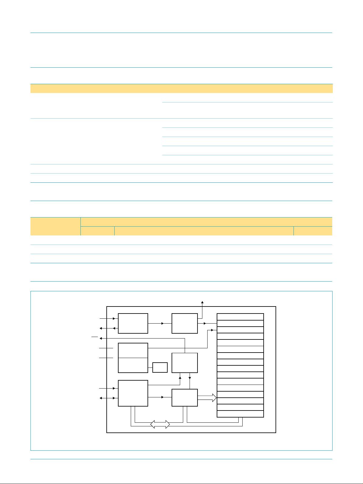
8. Functional description
The PCF8563 contains sixteen 8-bit registers with an auto-incrementing address
register, an on-chip 32.768 kHz oscillator with an integrated capacitor, a frequency
divider which provides the source clock for the Real-Time Clock (RTC), a
programmable clock output, a timer, an alarm, a voltage-low detector and a 400 kHz
I
2
C-bus interface.
All 16 registers are designed as addressable 8-bit parallel registers although not all
bits are implemented. The first two registers (memory address 00H and 01H) are
used as control and/or status registers. The memory addresses 02H through 08H are
used as counters for the clock function (seconds up to year counters). Address
locations 09H through 0CH contain alarm registers which define the conditions for an
alarm. Address 0DH controls the CLKOUT output frequency. 0EH and 0FH are the
timer control and timer registers, respectively.
The Seconds, Minutes, Hours, Days, Months, Years as well as the Minute alarm,
Hour alarm and Day alarm registers are all coded in BCD format. The Weekdays and
Weekday alarm register are not coded in BCD format.
When one of the RTC registers is read the contents of all counters are frozen.
Therefore, faulty reading of the clock/calendar during a carry condition is prevented.
8.1 Alarm function modes
By clearing the MSB (bit AE = Alarm Enable) of one or more of the alarm registers,
the corresponding alarm condition(s) will be active. In this way an alarm can be
generated from once per minute up to once per week. The alarm condition sets the
alarm flag, AF (bit 3 of Control/Status 2 register). The asserted AF can be used to
generate an interrupt (INT). Bit AF can only be cleared by software.
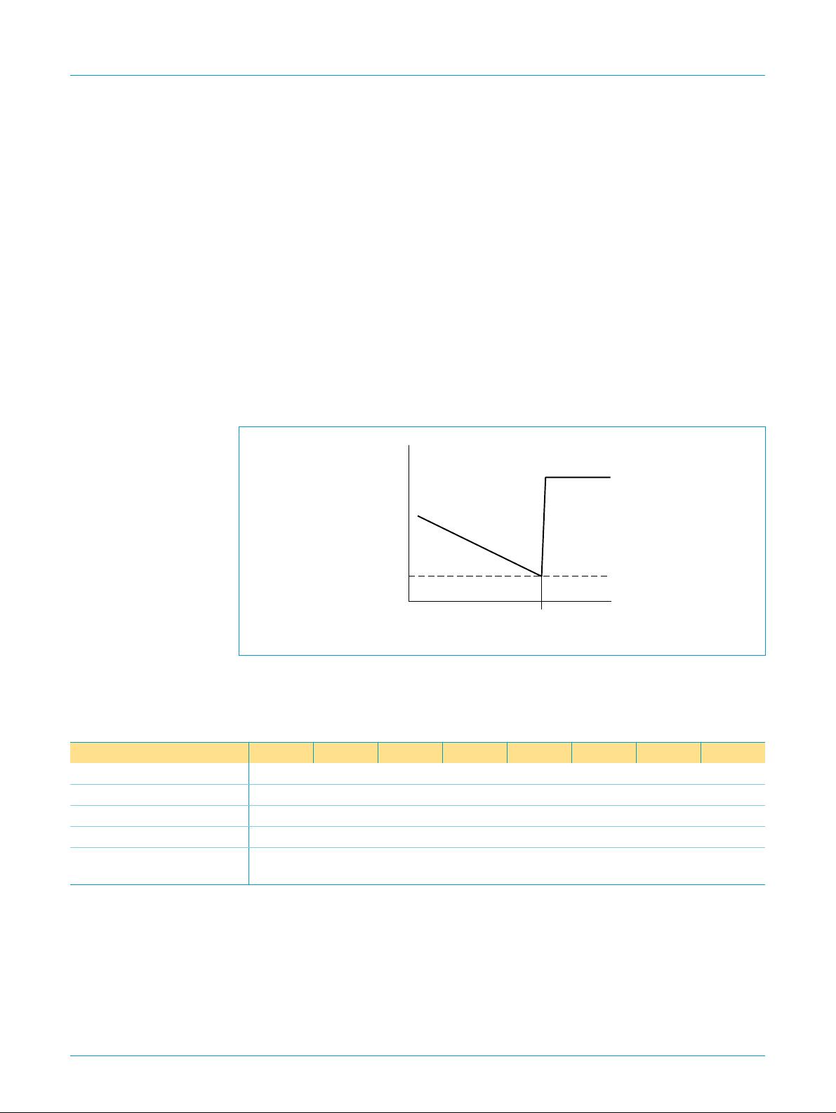
8.2 Timer
The 8-bit countdown timer (address 0FH) is controlled by the Timer Control register
(address 0EH; see Table 25). The Timer Control register selects one of 4 source
clock frequencies for the timer (4096, 64, 1, or
1
⁄
60
Hz), and enables/disables the
timer. The timer counts down from a software-loaded 8-bit binary value. At the end of
every countdown, the timer sets the timer flag TF (see Tabl e 7). The timer flag TF can
only be cleared by software. The asserted timer flag TF can be used to generate an
interrupt (INT). The interrupt may be generated as a pulsed signal every countdown
period or as a permanently active signal which follows the condition of TF. TI/TP (see
Table 7) is used to control this mode selection. When reading the timer, the current
countdown value is returned.
8.3 CLKOUT output
A programmable square wave is available at the CLKOUT pin. Operation is controlled
by the CLKOUT frequency register (address 0DH; see Tabl e 23). Frequencies of
32.768 kHz (default), 1024, 32 and 1 Hz can be generated for use as a system clock,
microcontroller clock, input to a charge pump, or for calibration of the oscillator.
CLKOUT is an open-drain output and enabled at power-on. If disabled it becomes
high-impedance.
Philips Semiconductors
PCF8563
Real-time clock/calendar
Product specification 16 April 1999 5 of 30
9397 750 04855
© Philips Electronics N.V. 1999. All rights reserved.
8.4 Reset
The PCF8563 includes an internal reset circuit which is active whenever the oscillator
is stopped. In the reset state the I
2
C-bus logic is initialized and all registers, including
the address pointer, are cleared with the exception of bits FE, VL, TD1, TD0, TESTC
and AE which are set to logic 1.
8.5 Voltage-low detector and clock monitor
The PCF8563 has an on-chip voltage-low detector. When V
DD
drops below V
low
the
VL bit (Voltage Low, bit 7 in the Seconds register) is set to indicate that reliable
clock/calendar information is no longer guaranteed. The VL flag can only be cleared
by software.
The VL bit is intended to detect the situation when V
DD
is decreasing slowly for
example under battery operation. Should V
DD
reach V
low
before power is re-asserted
then the VL bit will be set. This will indicate that the time may be corrupted.
8.6 Register organization
Fig 4. Voltage-low detection.
handbook, halfpage
VL set
normal power
operation
period of battery
operation
t
V
DD
V
low
MGR887
Table 4: Registers overview
Bit positions labelled as ‘
−
’are not implemented; those labelled with ‘0’ should always be written with logic 0.
Address Register name Bit 7 Bit 6 Bit 5 Bit 4 Bit 3 Bit 2 Bit 1 Bit 0
00H Control/Status 1 TEST1 0 STOP 0 TESTC 0 0 0
01H Control/Status 2 0 0 0 TI/TP AF TF AIE TIE
0DH CLKOUT frequency FE −−−−−FD1 FD0
0EH Timer control TE −−−−−TD1 TD0
0FH Timer countdown
value
<timer countdown value>
剩余29页未读,继续阅读
donkeylunzi
- 粉丝: 1
- 资源: 4
上传资源 快速赚钱
- 我的内容管理 展开
- 我的资源 快来上传第一个资源
- 我的收益 登录查看自己的收益
- 我的积分 登录查看自己的积分
- 我的C币 登录后查看C币余额
- 我的收藏
- 我的下载
- 下载帮助
安全验证
文档复制为VIP权益,开通VIP直接复制
信息提交成功
评论0