没有合适的资源?快使用搜索试试~ 我知道了~
RT5350_Preliminary_Datasheet RT5350 数据手册
5星 · 超过95%的资源 需积分: 42 33 下载量 23 浏览量
2013-06-30
06:40:39
上传
评论 1
收藏 9.49MB PDF 举报
温馨提示
试读
219页
RT5350_Preliminary_Datasheet RT5350 数据手册
资源推荐
资源详情
资源评论
RT5350
Preliminary Datasheet
PreliminaryDatNovember 25, 2010
DSRT5350_V1.0_112510
-1-
Form No.:QS-073-F02
Rev.:1
Kept by: DCC
Ret. Time: 5 Years
Introduction
The RT5350 SoC combines Ralink’s IEEE 802.11n draft compliant 1T1R MAC/BBP/PA/RF, a high
performance 360 MHz MIPS24KEc CPU core, a 5-port integrated 10/100 Ethernet switch/PHY and a USB
host/device. With the RT5350, there are very few external components required for 2.4 GHz 802.11n
wireless products. The RT5350 employs Ralink’s 2nd generation 802.11n technologies for longer range
and better throughput. The embedded, high performance CPU can easily manage advanced applications
such as Wi-Fi data processing without overloading the host processor. In addition, the RT5350 offers a
variety of hardware interfaces (SPI/I
2
S/I
2
C/PCM/UART/USB) to support a range of possible applications.
Applications
iNIC AP/Router
Features
Embedded 1T1R 2.4G CMOS RF
Embedded 802.11n 1T1R MAC/BBP with
MLD enhancement
Embedded PA/LNA
150 Mbps PHY data rate
20 Mhz/40 MHz channel width
Legacy and high throughout modes
Compressed block ACK
Bluetooth Co-existence
Multiple BSSID (up to 16)
WEP64/128, WPA, WPA2, WAPI engines
QOS - WMM, WMM Power Save
Hardware frame aggregation
Supports 802.11h TPC
MIPS 24KEc 360 Mhz with 32 KB I cache/16
KB D cache
Supports 16-bit SDR SDRAM (up to 64 MB)
Supports boot from ROM, FLASH
USB 2.0 HOST/Device dual mode x1
Embedded 5-port 10/100 Mbps Ethernet
switch and 5-port UTP PHY
Supports 5 10/100 UTP ports
Slow speed I/O : GPIO, SPI, I
2
C, I
2
S, PCM,
UART, and JTAG
Packaging and I/O voltage
12 mm x 12 mm TFBGA-196 package
I/O: 3.3 V I/O
Functional Block Diagram
Order Information
Ralink Technology Corp. (USA)
Suite 200
20833 Stevens Creek Blvd.
Cupertino, CA95014
Tel: 408-725-8070
Fax: 408-725-8069
Ralink Technology Corp. (Taiwan)
5F. 36 Taiyuan St,
Jhubei City, Hsin-Chu
Taiwan, R.O.C
Tel: 886-3-560-0868
Fax: 886-3-560-0818
Part
Number
Temp
Range
Packaging
RT5350F
-10~
55
0
C
Green/RoHS
Compliant
TFBGA 196 ball
(12 mm x 12
mm)
MIPS 24KEc
(360 MHz)
32K I
-
Cache
16K D
-
Cache
Clock/Timer/Reset/PLL
802.11n
1T1R
MAC
BBP
802.11n
1T1R
2.4 GHz
RF
1T2R
Diversity
SDRAM/
Controller
PCM
SPI
I
2
S
I
2
C
USB 2.0
Host/Device PHY
UART Full+Lite
External Interface
40/20 MHz
Crystall
FE
Router
Transform
er
16bit SDRAM
UART Interface
USB 2.0 Interface
EEPROM/Control
Audio Interface
SLIC
Codec
GPIO/LED
0
1
2
3
4
Fast Ethernet Switch
Draft
RT5350
Preliminary Datasheet
PreliminaryDatNovember 25, 2010
DSRT5350_V1.0_112510
-2-
Form No.:QS-073-F02
Rev.:1
Kept by: DCC
Ret. Time: 5 Years
Table of Contents
INTRODUCTION ....................................................................................................................................................... 1
1 PIN DESCRIPTION .......................................................................................................................................... 6
1.1 196-PIN BGA PACKAGE DIAGRAM .................................................................................................................. 6
1.2 PIN DESCRIPTION .......................................................................................................................................... 6
1.3 PIN SHARING SCHEME .................................................................................................................................. 12
1.4 BOOT STRAPPING DESCRIPTION ...................................................................................................................... 14
2 MAXIMUM RATINGS AND OPERATING CONDITIONS (TBD) ........................................................................ 15
2.1 ABSOLUTE MAXIMUM RATINGS ..................................................................................................................... 15
2.2 THERMAL INFORMATION .............................................................................................................................. 15
2.3 OPERATING CONDITIONS .............................................................................................................................. 15
2.4 STORAGE CONDITION ................................................................................................................................... 15
2.5 EXTERNAL XTAL SPECFICATIONS ..................................................................................................................... 15
2.6 DC ELECTRICAL CHARACTERISTICS .................................................................................................................. 15
2.7 AC ELECTRICAL CHARACTERISTICS ................................................................................................................... 15
2.7.1 SDRAM Interface ........................................................................................................................... 16
2.7.2 Power On Sequence ...................................................................................................................... 17
3 FUNCTION DESCRIPTION ............................................................................................................................. 18
3.1 OVERVIEW ................................................................................................................................................. 18
3.2 MEMORY MAP SUMMARY ............................................................................................................................ 19
3.3 MIPS 24 KBPS PROCESSOR .......................................................................................................................... 20
3.3.1 Features ........................................................................................................................................ 20
3.3.2 Block Diagram ............................................................................................................................... 21
3.3.3 Clock Plan ...................................................................................................................................... 21
3.4 SYSTEM CONTROL ....................................................................................................................................... 22
3.4.1 Features ........................................................................................................................................ 22
3.4.2 Block Diagram ............................................................................................................................... 22
3.4.3 Register Description (base: 0x1000_0000) ................................................................................... 22
3.4.4 TIMER (TBD)......................................................................................................................................... 31
3.4.5 Features ........................................................................................................................................ 31
3.4.6 Block Diagram ............................................................................................................................... 33
3.4.7 Register Description (base: 0x1000_0100) .................................................................................. 33
3.5 INTERRUPT CONTROLLER ............................................................................................................................... 37
3.5.1 Features ........................................................................................................................................ 37
3.5.2 Block Diagram ............................................................................................................................... 37
3.5.3 Register Description (base: 0x1000_0200) ................................................................................... 37
3.6 SYSTEM TICK COUNTER ................................................................................................................................ 42
3.6.1 Register Description (base: 0x1000_0d00) ................................................................................... 42
3.7 UART ....................................................................................................................................................... 43
3.7.1 Features ........................................................................................................................................ 43
3.7.2 Block Diagram ............................................................................................................................... 43
3.7.3 Register Description (base: 0x1000_0500) ................................................................................... 43
3.8 UART LITE ................................................................................................................................................ 50
3.8.1 Features ........................................................................................................................................ 50
3.8.2 Block Diagram ............................................................................................................................... 50
3.8.3 Register Description (base: 0x1000_0c00) .................................................................................... 50
3.9 PROGRAMMABLE I/O .................................................................................................................................. 56
3.9.1 Features ........................................................................................................................................ 56
3.9.2 Block Diagram ............................................................................................................................... 56
3.9.3 Register Description (base: 0x1000_0600) ................................................................................... 56
3.10 I
2
C CONTROLLER .................................................................................................................................... 62
3.10.1 Features ................................................................................................................................... 62
3.10.2 Block Diagram .......................................................................................................................... 62
Draft
RT5350
Preliminary Datasheet
PreliminaryDatNovember 25, 2010
DSRT5350_V1.0_112510
-3-
Form No.:QS-073-F02
Rev.:1
Kept by: DCC
Ret. Time: 5 Years
3.10.3 Register Description (base: 0x1000_0900) ............................................................................... 62
3.10.4 Programming Description ........................................................................................................ 66
3.11 PCM CONTROLLER ................................................................................................................................. 68
3.11.1 Features ................................................................................................................................... 68
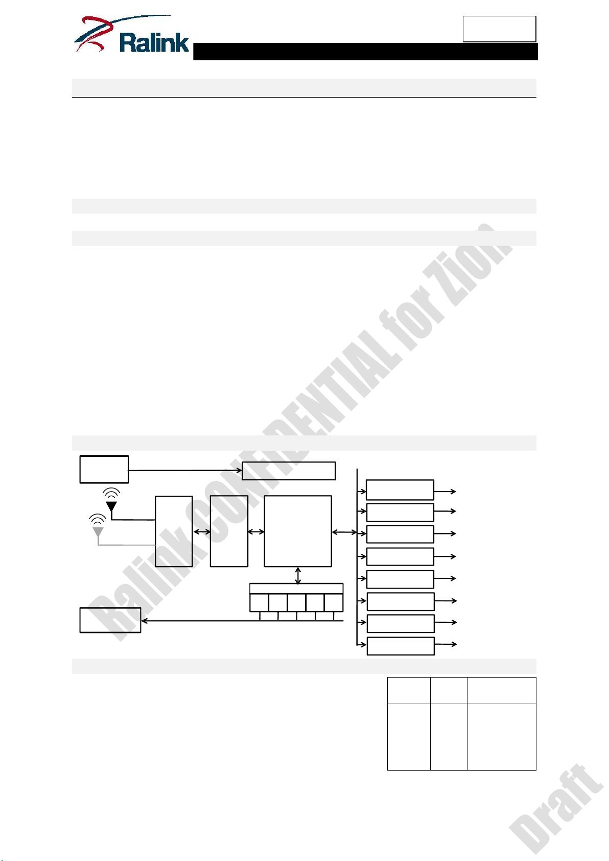
3.11.2 Block Diagram .......................................................................................................................... 68
3.11.3 Register Description (base: 0x1000_2000) ............................................................................... 69
3.11.4 An Example of PCM Configuration ........................................................................................... 75
3.12 GENERIC DMA CONTROLLER .................................................................................................................... 77
3.12.1 Features ................................................................................................................................... 77
3.12.2 Block Diagram .......................................................................................................................... 77
3.12.3 Peripheral Channel Connection ................................................................................................ 77
3.12.4 Register Description (base: 0x1000_2800) ............................................................................... 78
3.13 SPI CONTROLLER .................................................................................................................................... 82
3.13.1 Features ................................................................................................................................... 82
3.13.2 Block Diagram .......................................................................................................................... 82
3.13.3 Register Description (base: 0x1000_0b00) ............................................................................... 82
3.14 I
2
S CONTROLLER .................................................................................................................................... 88
3.14.1 Features ................................................................................................................................... 88
3.14.2 Block Diagram .......................................................................................................................... 88
3.14.3 I
2
S Signal Timing for I
2
S Data Format ....................................................................................... 88
3.14.4 Register Description of I
2
S (base: 0x1000_0a00) ..................................................................... 89
3.15 MEMORY CONTROLLER ............................................................................................................................ 92
3.15.1 Features ................................................................................................................................... 92
3.15.2 Block Diagram .......................................................................................................................... 92
3.15.3 SDRAM Initialization Sequence ................................................................................................ 92
3.15.4 Register Description (base: 0x1000_0300) ............................................................................... 93
3.16 USB HOST CONTROLLER & PHY ............................................................................................................... 97
3.16.1 Features ................................................................................................................................... 97
3.16.2 Block Diagram .......................................................................................................................... 97
3.16.3 Register Description (base: 0x101c_0000) ............................................................................... 97
3.16.4 EHCI Operation register (base: 0x101c_0000) ......................................................................... 97
3.16.5 OHCI Operation register (base: 0x101c_1000) ......................................................................... 99
3.17 USB DEVICE CONTROLLER...................................................................................................................... 100
3.17.1 Features ................................................................................................................................. 100
3.17.1.1 PDMA Descriptor Format .................................................................................................................. 100
3.17.1.2 Bulk-out Aggregation Format ............................................................................................................ 101
3.17.2 Register Description (base: 0x1012_0000) ............................................................................. 102
3.17.2.1 USB Control Registers ....................................................................................................................... 102
3.17.2.2 UDMA Registers ................................................................................................................................ 102
3.17.2.3 PDMA Registers ................................................................................................................................ 102
3.18 FRAME ENGINE .................................................................................................................................... 108
3.18.1 Features ................................................................................................................................. 108
3.18.2 Block Diagram ........................................................................................................................ 108
3.18.2.1 PDMA FIFO-like Ring Concept ........................................................................................................... 109
3.18.2.2 PDMA Descriptor Format .................................................................................................................. 110
3.18.3 PDMA Register Description (base: 0x1010_0800) .................................................................. 110
3.18.4 SDM Register Description (base: 0x1010_0c00) .................................................................... 115
3.19 ETHERNET SWITCH ................................................................................................................................ 120
3.19.1 Features ................................................................................................................................. 120
3.19.2 Block Diagram ........................................................................................................................ 121
3.19.3 Frame Classification ............................................................................................................... 121
3.19.4 Register Description (base: 0x1011_0000) ............................................................................. 122
3.19.5 MII Control Register ............................................................................................................... 156
3.19.6 Function Description .............................................................................................................. 160
3.19.6.1 Flow Control Settings ........................................................................................................................ 160
3.19.6.2 VID and Tagging ................................................................................................................................ 160
3.19.6.3 VID and VLAN Member Set ............................................................................................................... 160
Draft
RT5350
Preliminary Datasheet
PreliminaryDatNovember 25, 2010
DSRT5350_V1.0_112510
-4-
Form No.:QS-073-F02
Rev.:1
Kept by: DCC
Ret. Time: 5 Years
3.19.6.4 Packet Classification, QoS, Scheduling and Buffer Control ............................................................... 162
3.19.6.5 Spanning Tree Protocol ..................................................................................................................... 163
3.20 802.11N 1T1R MAC/BBP ................................................................................................................... 165
3.20.1 Features ................................................................................................................................. 165
3.20.2 Block Diagram ........................................................................................................................ 165
3.20.3 Register Description - SCH/WPDMA (base: 0x1018_0000) .................................................... 166
3.20.3.1 Register Description - PBF (base: 0x1018_0000) .............................................................................. 172
3.20.3.2 Register Description – RF TEST (base: 0x1018_0000) ....................................................................... 177
3.20.3.3 Register Description - MAC (base: 0x1018_0000) ............................................................................. 178
3.20.3.4 MAC Tx Configuration Registers (offset: 0x1300) ............................................................................. 186
3.20.3.5 MAC Rx Configuration Registers ....................................................................................................... 197
3.20.3.6 MAC Security Configuration Registers .............................................................................................. 199
3.20.3.7 MAC HCCA/PSMP CSR ....................................................................................................................... 199
3.20.3.8 MAC Statistics Counters .................................................................................................................... 201
3.20.3.9 MAC Search Table (base: 0x1018_0000, offset: 0x1800) .................................................................. 203
3.20.3.10 Security table/CIS/Beacon/NULL frame (base : 1018_0000, offset: 0x4000) .................................... 204
3.20.4 Security Key Format (8DW) .................................................................................................... 204
3.20.5 IV/EIV Format (2 DW) ............................................................................................................. 204
3.20.6 WCID Attribute Entry Format (1DW) ...................................................................................... 204
3.20.7 Shared Key Mode Entry Format (1DW) .................................................................................. 205
3.20.7.1 Security Tables .................................................................................................................................. 205
3.20.8 Descriptor and Wireless information ..................................................................................... 207
3.20.8.1 Tx Frame Information ....................................................................................................................... 207
3.20.8.2 Tx Descriptor Format ........................................................................................................................ 207
3.20.8.3 TXWI Format ..................................................................................................................................... 209
3.20.8.4 Rx Descriptor Ring ............................................................................................................................. 210
3.20.8.5 RX Descriptor Format ........................................................................................................................ 211
3.20.8.6 RXWI Format ..................................................................................................................................... 212
3.20.8.7 Brief PHY Rate Format and Definition ............................................................................................... 212
3.20.9 Driver Implementation Note .................................................................................................. 214
3.20.9.1 Instructions for Downloading 8051 Firmware .................................................................................. 214
3.20.9.2 Instructions for Initializing DMA ....................................................................................................... 214
3.20.9.3 Instructions for Clock Control ........................................................................................................... 214
3.20.9.4 Instructions for Tx/Rx Control ........................................................................................................... 215
3.20.9.5 Instructions for RF Power on/off Sequence ...................................................................................... 215
3.20.9.6 Power Saving Procedure ................................................................................................................... 216
3.20.9.7 Power Recovery Procedure ............................................................................................................... 216
3.20.9.8 Parameters ........................................................................................................................................ 216
4 PACKAGING PHYSICAL DIMENSIONS ......................................................................................................... 217
4.1 TFBGA 196B(12×12×0.94 MM) ......................................................................................................... 217
5 REVISION HISTORY .................................................................................................................................... 219
Draft
RT5350
Preliminary Datasheet
PreliminaryDatNovember 25, 2010
DSRT5350_V1.0_112510
-5-
Form No.:QS-073-F02
Rev.:1
Kept by: DCC
Ret. Time: 5 Years
Table of Figures
FIGURE 2-1 SDRAM INTERFACE .................................................................................................................................. 16
FIGURE 2-2 POWER-ON SEQUENCE .............................................................................................................................. 17
FIGURE 3-1 RT5350 BLOCK DIAGRAM ......................................................................................................................... 18
FIGURE 3-2 MIPS 24KEC PROCESSOR DIAGRAM ............................................................................................................ 21
FIGURE 3-3 SYSTEM CONTROL BLOCK DIAGRAM ............................................................................................................. 22
FIGURE 3-4 TIMER BLOCK DIAGRAM ............................................................................................................................. 33
FIGURE 3-5 INTERRUPT CONTROLLER BLOCK DIAGRAM .................................................................................................... 37
FIGURE 3-6 UART BLOCK DIAGRAM ............................................................................................................................. 43
FIGURE 3-7 UART LITE BLOCK DIAGRAM ...................................................................................................................... 50
FIGURE 3-8 PROGRAM I/O BLOCK DIAGRAM .................................................................................................................. 56
FIGURE 3-9 1 I
2
C CONTROLLER BLOCK DIAGRAM ............................................................................................................ 62
FIGURE 3-10 PCM CONFIGURATION EXAMPLE 1 ............................................................................................................ 75
FIGURE 3-11 PCM CONFIGURATION EXAMPLE 2 ............................................................................................................ 76
FIGURE 3-12 PCM CONFIGURATION EXAMPLE 3 ............................................................................................................ 76
FIGURE 3-13 GENERIC DMA CONTROLLER BLOCK DIAGRAM ............................................................................................. 77
FIGURE 3-14 SPI CONTROLLER BLOCK DIAGRAM ............................................................................................................ 82
FIGURE 3-15 WAVEFORM OF SPI INTERFACE .................................................................................................................. 87
FIGURE 3-16 I
2
S TRANSMITTER BLOCK DIAGRAM ............................................................................................................ 88
FIGURE 3-17 I
2
S TRANSMITTER/RECEIVER ..................................................................................................................... 88
FIGURE 3-18 SRAM/SDRAM CONTROLLER BLOCK DIAGRAM .......................................................................................... 92
FIGURE 3-19 USB HOST CONTROLLER & PHY BLOCK DIAGRAM ........................................................................................ 97
FIGURE 3-20 PDMA TX DESCRIPTOR FORMAT ............................................................................................................. 100
FIGURE 3-21 PDMA RX DESCRIPTOR FORMAT ............................................................................................................. 101
FIGURE 3-22 BULK-OUT AGGREGATION FORMAT .......................................................................................................... 101
FIGURE 3-23 FRAME ENGINE BLOCK DIAGRAM ............................................................................................................. 108
FIGURE 3-24 PDMA FIFO-LIKE RING CONCEPT ........................................................................................................... 109
FIGURE 3-25 PDMA TX DESCRIPTOR FORMAT ............................................................................................................. 110
FIGURE 3-26 PDMA RX DESCRIPTOR FORMAT ............................................................................................................. 110
FIGURE 3-27 ETHERNET SWITCH BLOCK DIAGRAM ........................................................................................................ 121
FIGURE 3-28 DOUBLE TAG ........................................................................................................................................ 161
FIGURE 3-29 SPECIAL TAG ........................................................................................................................................ 161
FIGURE 3-30 PACKET CLASSIFICATION, QOS, SCHEDULING, AND BUFFER CONTROL ............................................................. 163
FIGURE 3-31 802.11N 1T1R MAC/BBP BLOCK DIAGRAM ........................................................................................... 165
FIGURE 3-32 802.11N 3T3R MAC/BBP REGISTER MAP ............................................................................................. 166
FIGURE 3-33 TX FRAME INFORMATION ....................................................................................................................... 207
FIGURE 3-34 TX DESCRIPTOR FORMAT ........................................................................................................................ 208
FIGURE 3-35 TXWI FORMAT .................................................................................................................................... 209
FIGURE 3-36 RX DESCRIPTOR RING ............................................................................................................................ 210
FIGURE 3-37 RX DESCRIPTOR FORMAT ........................................................................................................................ 211
FIGURE 3-38 RXWI FORMAT .................................................................................................................................... 212
Draft
剩余218页未读,继续阅读
资源评论
- yoe_cho2013-08-29是RT5350的资料,但是5分太贵
- xiaoyao_412014-04-09是RT5350的资料,但是5分太贵
- star_999_xing2018-04-17很有用的,正需要
- royrobin6862013-10-23怎么9M的文档和5M的文档一样的内容,5分贵了点,文档还是不错的
csdddn
- 粉丝: 12
- 资源: 209
上传资源 快速赚钱
- 我的内容管理 展开
- 我的资源 快来上传第一个资源
- 我的收益 登录查看自己的收益
- 我的积分 登录查看自己的积分
- 我的C币 登录后查看C币余额
- 我的收藏
- 我的下载
- 下载帮助
安全验证
文档复制为VIP权益,开通VIP直接复制
信息提交成功