没有合适的资源?快使用搜索试试~ 我知道了~
cxd3142 pdf
5星 · 超过95%的资源 需积分: 10 19 下载量 63 浏览量
2010-11-25
15:22:47
上传
评论
收藏 671KB PDF 举报
温馨提示
试读
58页
cxd3142 Signal Processor LSI for Single-Chip CCD Color Camera
资源推荐
资源详情
资源评论
– 1 –
E02523-PS
Sony reserves the right to change products and specifications without prior notice. This information does not convey any license by
any implication or otherwise under any patents or other right. Application circuits shown, if any, are typical examples illustrating the
operation of the devices. Sony cannot assume responsibility for any problems arising out of the use of these circuits.
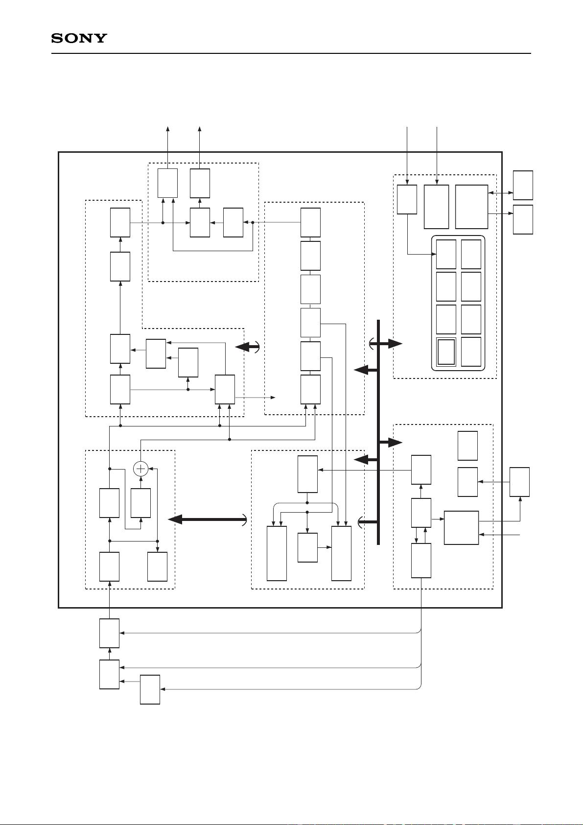
CXD3142R
80 pin LQFP (Plastic)
Signal Processor LSI for Single-Chip CCD Color Camera
Description
The CXD3142R is a signal processor LSI for Ye,
Cy, Mg and G single-chip CCD color cameras. In
addition to basic camera signal processing functions,
it includes an AE/AWB detection circuit, a sync signal
generation circuit and an external sync circuit, etc.
This chip also has a built-in microcontroller to realize
basic camera functions such as AE/AWB without an
external microcomputer.
Features
• Generates timing pulses to drive the 510H CCD
image sensor
Sync signal generation function
Luminance/chroma signal processing
Luminance/chroma signal integral detector
Automatically control camera function
• Supports NTSC/PAL modes
• Supports 510H system CCD image sensor
• Built-in 9-bit A/D converter
• Analog composite output
— Built-in digital encoder
— 10-bit D/A converter output
• Digital output
— YUV 8-bit multiplex output
• Supports external sync functions
• AE/AWB detector
• Block control functions with a built-in microcontroller
— AE/AWB/YC/CLAMP/SG control functions
• Peripheral IC communication control functions
— EVR, EEPROM communication control
• Serial communication function
— Microcomputer (3 wires)
Absolute Maximum Ratings
• Supply voltage VDD VSS – 0.5 to +4.6 V
AVDD VSS – 0.5 to +4.6 V
• Input voltage VI VSS – 0.5 to VDD + 0.5 V
• Output voltage VO VSS – 0.5 to VDD + 0.5 V
• Operating temperature
Topr –20 to + 75 °C
• Storage temperature
Tstg –55 to +150 °C
Recommended Operating Conditions
• Supply voltage VDD 3.0 to 3.6 V
AVDD (AVD1, 2, 5, 6) 3.0 to 3.6 V
AVDD (AVD4) 3.0 to 5.5 V
• Operating temperature
Topr –20 to +75°C
Applications
• Industrial CCD cameras
(surveillance/FA/image input cameras)
• Multimedia CCD cameras
(teleconferencing/personal computer cameras)
Applicable CCD Image Sensors
∗
510H color CCDs (Type 1/3, 1/4, 1/6 NTSC/PAL)
Supported Relates LSIs
V-Driver: CXD1267AN
AGC: CXA2096N
EVR: MB88347 (Fujitsu Limited.)
EEPROM: CAT64LC40JI
(Catalyst Semiconductor Inc.)
AK6420
(Asahi Kasei Microsystems Co.,Ltd.)
∗
Applicable CCD Image Sensors are applicable products as of
preparing this data sheet.
They may be changed according to the version up and production
stop of CCD image sensor.
– 2 –
CXD3142R
Block Diagram
CXD1267AN
CXA2096N
CCD
V-DRV
CDS
AGC
CXD3142R
PRE
A/D
1HDL
1HDL
OB
DET
Y-Process
LPF
CLMP
GAM GAIN
BLK
DADJ
HV
APC
H
APC
V
APC
VSPRS/
HSPRS
YCmix
YC-
MIX
YC-
MPX
D/A
Analog
Composite
Digital
YUV
D-ENC
C-Process
LPF
CLMP
RGB
MTX
WB GAM
LN
MTX
DADJ
DIP_SW
External µcom
CPU
Software
SYS
CON
INIT
CLAMP
PORT
DRV
SG
YC
CTRL
AE
AWB
PORT
EXT-SIF
• µCOM
CAM-SIF
• EVR
• EEPROM
EVR
EEP
ROM
OPD
Y-INTG
REF
GATE
WEIGHT
GEN
RGB-CNT
RGB-INTG
STG
Y-AE
C-WB
TIMING
GEN
SYNC
GEN
WIND
GEN
VD
V
PHASE
COMP
PLL
OSC
OSC
PLL
LPF
V cycle sig
– 3 –
CXD3142R
Pin Configuration
1 2 3 4 5 6 7 8 9 10 11 12 13 14 15
16
17 18 19 20
21
22
23
24
25
26
27
28
29
30
31
32
33
34
35
36
37
38
39
40
42434445464748495051525354555657585960
61
62
63
64
65
66
67
68
69
70
71
72
73
74
75
76
77
78
79
80
VRT
AVD1
VIN
AVS1
VRB
XSHP
XSHD
AVD2
XRS
AVS2
RG
REFC3
AVD4
H2
H1
AVS3
V
SS1
XSUB
V
DD1
XV1
PCOMP
SCK
SO
SI
XCS
V
DD2
CASCK
CASO
CASI
CSROM
CSEVR
V
SS2
PCK
PSCO
PSCI
XSG2
XV4
XV3
XSG1
XV2
D7
D6
D5
D4
D3
D2
D1
D0
AVD6
S0 (FLD)
S1 (VD)
S2 (HD)
XRST
V
DD4
NTPAL
TEST
V
SS4
PBLK
CLPDM
CLP0
IO
AVD5
VG
VREF
IREF
AVS5
VB
V
SS3
P7 (AWB3)
P6 (AWB2)
P5 (AWB1)
P4 (SHTFIX)
P3 (AGCMAX)
P2 (BLCOFF)
P1 (MIRIS)
P0 (AEME)
V
DD3
CK
OSCO
41
OSCI
Note) Symbols in parentheses are the signal names when the LSI is switched by the serial communication
settings.
All pin symbols (pin names) for the CXD3142R are the names next to the pin No. (outside the
parentheses).
– 4 –
CXD3142R
Pin Description
Pin
No.
Symbol I/O Description
Power
supply
1
2
3
4
5
6
7
8
9
10
11
12
13
14
15
16
17
18
19
20
21
22
23
24
25
26
27
28
29
30
31
32
33
34
35
VRT
AVD1
VIN
AVS1
VRB
XSHP
XSHD
AVD2
XRS
AVS2
RG
REFC3
AVD4
H2
H1
AVS3
VSS1
XSUB
VDD1
XV1
XV2
XSG1
XV3
XV4
XSG2
PSCI
PSCO
PCK
VSS2
CSEVR
CSROM
CASI
CASO
CASCK
VDD2
I (A)
—
I (A)
—
I (A)
O
O
—
O
—
O
I
—
O
O
—
—
O
—
O
O
O
O
O
O
I
O
I
—
O
O
I
O
O
—
A/D converter reference voltage (top) input.
Power supply for A/D converter. (+3.3V)
A/D converter analog signal input.
GND
A/D converter reference voltage (bottom) input.
Precharge level sample-and-hold pulse output.
Data sample-and-hold pulse output.
Power supply for sample-and-hold pulse driver. (+3.3V)
Resampling pulse output.
GND
Reset gate pulse output.
Reference capacitor connection pin.
Power supply for H driver. (+3.3V/+5.0V)
CCD horizontal register transfer pulse output.
GND
GND
CCD electronic shutter pulse output.
Power supply for Logic. (+3.3V)
CCD vertical register transfer pulse output.
CCD sensor readout pulse output.
CCD vertical register transfer pulse output.
CCD sensor readout pulse output.
Oscillation cell input. (slave)
Oscillation cell output. (slave)
System clock input. (slave)
GND
Chip select output for camera peripheral ICs. (to EVR)
Chip select output for camera peripheral ICs. (to EEPROM)
Serial data input for camera peripheral ICs. (from EEPROM)
Serial data output for camera peripheral ICs. (to EVR, EEPROM)
Serial clock output for camera peripheral ICs. (to EVR, EEPROM)
Power supply for Logic. (+3.3V)
AVD1
AVD2
AVD4
VDD
A/DS/HCCDOSC2
Peripheral
communication
– 5 –
CXD3142R
Pin
No.
Symbol I/O Description
Power
supply
36
37
38
39
40
41
42
43
44
45
46
47
48
49
50
51
52
53
54
55
56
57
58
59
60
61
62
63
64
65
66
67
68
69
XCS
SI
SO
SCK
PCOMP
OSCI
OSCO
CK
VDD3
P0 (AEME)
P1 (MIRIS)
P2 (BL COFF)
P3 (AGCMAX)
P4 (SHTFIX)
P5 (AWB1)
P6 (AWB2)
P7 (AWB3)
VSS3
VB
AVS5
IREF
VREF
VG
AVD5
IO
D7
D6
D5
D4
D3
D2
D1
D0
AVD6
I
I
O
I
O/Z
I
O
I
—
I
I
I
I
I
I
I
I
—
I (A)
—
O (A)
I (A)
I (A)
—
O
O/Z
O/Z
O/Z
O/Z
O/Z
O/Z
O/Z
O/Z
—
Chip select input for microcomputer communication.
Serial data input for microcomputer communication.
Serial data output for microcomputer communication.
Serial clock input for microcomputer communication.
Phase comparator output for PLL.
Oscillation cell input. (master)
Oscillation cell output. (master)
System clock input. (master)
Power supply for Logic. (+3.3V)
Port 0 input for mode switch. (AE mode switching)
Port 1 input for mode switch. (Iris mode switching)
Port 2 input for mode switch. (Backlight compensation off)
Port 3 input for mode switch. (AGC maximum gain switching)
Port 4 input for mode switch. (SHUT FIX mode switching)
Port 5 input for mode switch. (AWB mode switching)
Port 6 input for mode switch. (ATW/push lock switching)
Port 7 input for mode switch. (Push lock signal input )
GND
Capacitor connection pin. (about 0.1µF)
GND
Reference current setting pin.
Reference voltage setting pin.
Capacitor connection pin. (about 0.1µF)
Power supply for D/A converter. (+3.3V)
Composite signal (current) output.
Digital signal output.
Power supply for A/D converter. (+3.3V)
VDD
AVD5
VDD
External
communication
OSC1SWD/ADigital output
剩余57页未读,继续阅读
资源评论
- hs138221042015-04-21不错,确实有用!摄像头上的常见芯片。
cs163emai
- 粉丝: 0
- 资源: 6
上传资源 快速赚钱
- 我的内容管理 展开
- 我的资源 快来上传第一个资源
- 我的收益 登录查看自己的收益
- 我的积分 登录查看自己的积分
- 我的C币 登录后查看C币余额
- 我的收藏
- 我的下载
- 下载帮助
安全验证
文档复制为VIP权益,开通VIP直接复制
信息提交成功