Data Sheet
©2003 Silicon Storage Technology, Inc.
S71145-03-000 3/03 399
1
The SST logo and SuperFlash are registered trademarks of Silicon Storage Technology, Inc.
MPF is a trademark of Silicon Storage Technology, Inc.
These specifications are subject to change without notice.
16 Mbit (x16) Multi-Purpose Flash
SST39LF160 / SST39VF160
FEATURES:
• Organized as 1M x16
• Single Voltage Read and Write Operations
– 3.0-3.6V for SST39LF160
– 2.7-3.6V for SST39VF160
• Superior Reliability
– Endurance: 100,000 Cycles (typical)
– Greater than 100 years Data Retention
• Low Power Consumption
(typical values at 14 MHz)
– Active Current: 12 mA (typical)
– Standby Current: 4 µA (typical)
– Auto Low Power Mode: 4 µA (typical)
• Sector-Erase Capability
– Uniform 2 KWord sectors
• Fast Read Access Time
– 55 ns for SST39LF160
– 70 and 90 ns for SST39VF160
• Latched Address and Data
• Fast Erase and Word-Program
– Sector-Erase Time: 18 ms (typical)
– Block-Erase Time: 18 ms (typical)
– Chip-Erase Time: 70 ms (typical)
– Word-Program Time: 14 µs (typical)
– Chip Rewrite Time: 15 seconds (typical) for
SST39LF/VF160
• Automatic Write Timing
– Internal V
PP
Generation
• End-of-Write Detection
– Toggle Bit
– Data# Polling
• CMOS I/O Compatibility
• JEDEC Standard
– Flash EEPROM Pinouts and command sets
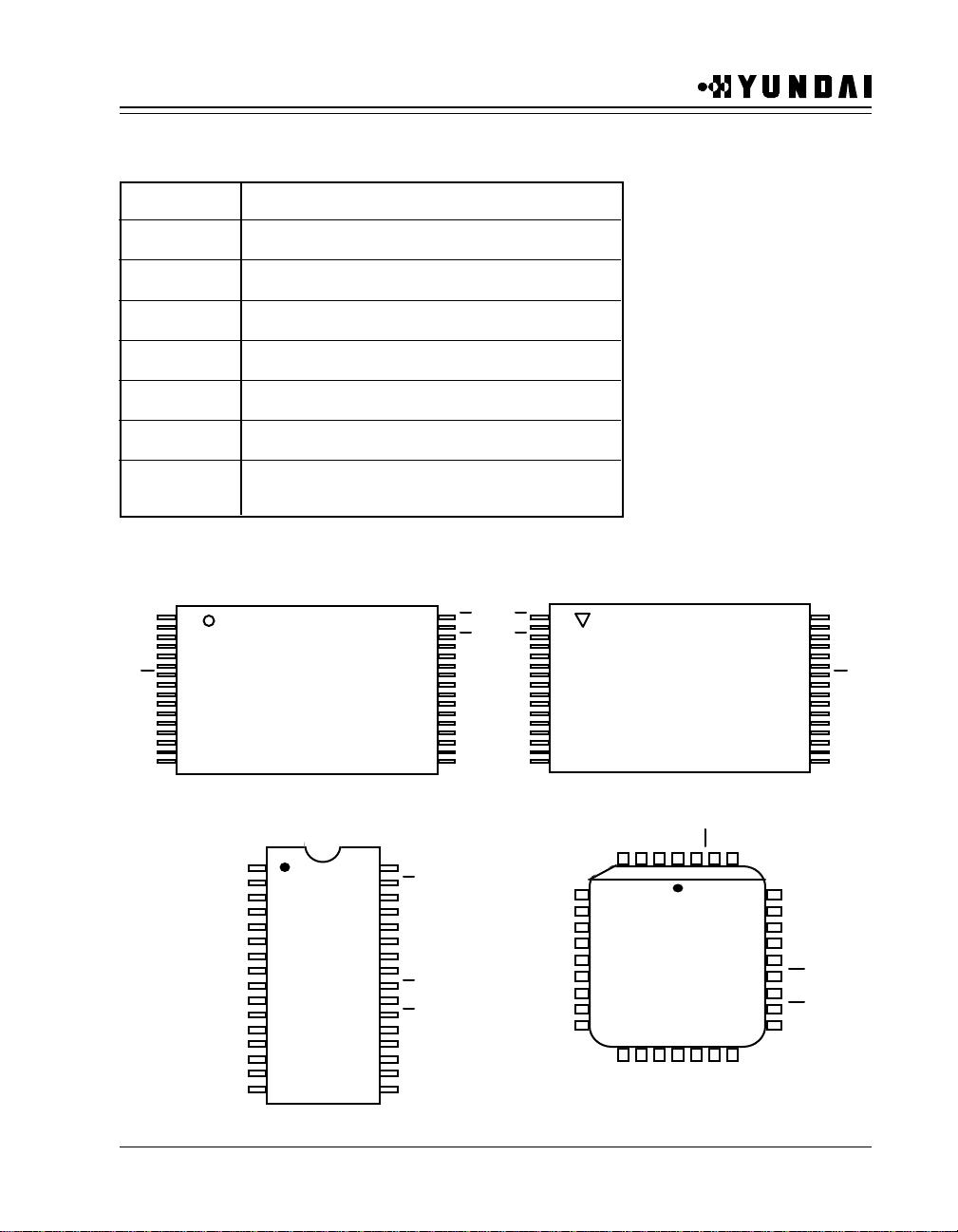
• Packages Available
– 48-lead TSOP (12mm x 20mm)
– 48-ball TFBGA (8mm x 10mm)
PRODUCT DESCRIPTION
The SST39LF/VF160 devices are 1M x16 CMOS Multi-
Purpose Flash (MPF) manufactured with SST’s propri-
etary, high performance CMOS SuperFlash technology.
The split-gate cell design and thick-oxide tunneling injec-
tor attain better reliability and manufacturability compared
with alternate approaches. The SST39LF160 write (Pro-
gram or Erase) with a 3.0-3.6V power supply. The
SST39VF160 write (Program or Erase) with a 2.7-3.6V
power supply. These devices conform to JEDEC standard
pinouts for x16 memories.
Featuring high performance Word-Program, the
SST39LF/VF160 devices provide a typical Word-Program
time of 14 µsec. These devices use Toggle Bit or Data#
Polling to indicate the completion of Program operation.
To protect against inadvertent write, they have on-chip
hardware and Software Data Protection schemes.
Designed, manufactured, and tested for a wide spectrum
of applications, these devices are offered with a guaran-
teed typical endurance of 10,000 cycles. Data retention is
rated at greater than 100 years.
The SST39LF/VF160 devices are suited for applications
that require convenient and economical updating of pro-
gram, configuration, or data memory. For all system appli-
cations, they significantly improve performance and
reliability, while lowering power consumption. They inher-
ently use less energy during Erase and Program than
alternative flash technologies. The total energy consumed
is a function of the applied voltage, current, and time of
application. Since for any given voltage range, the Super-
Flash technology uses less current to program and has a
shorter erase time, the total energy consumed during any
Erase or Program operation is less than alternative flash
technologies. These devices also improve flexibility while
lowering the cost for program, data, and configuration
storage applications.
The SuperFlash technology provides fixed Erase and Pro-
gram times, independent of the number of Erase/Program
cycles that have occurred. Therefore the system software
or hardware does not have to be modified or de-rated as
is necessary with alternative flash technologies, whose
Erase and Program times increase with accumulated
Erase/Program cycles.
To meet high density, surface mount requirements, the
SST39LF/VF160 are offered in a 48-lead TSOP and a
48-ball TFBGA package. See Figures 1 and 2 for pin
assignments.
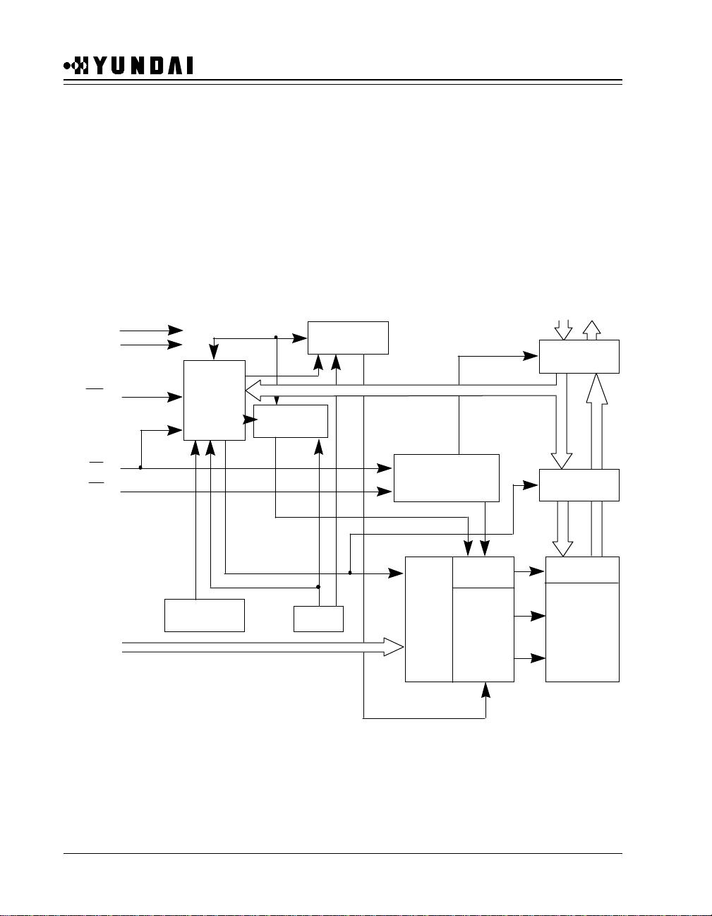
Device Operation
Commands are used to initiate the memory operation func-
tions of the device. Commands are written to the device
using standard microprocessor write sequences. A com-
mand is written by asserting WE# low while keeping CE#
low. The address bus is latched on the falling edge of WE#
or CE#, whichever occurs last. The data bus is latched on
the rising edge of WE# or CE#, whichever occurs first.
SST39LF/VF1603.0 & 2.7V 16Mb (x16) MPF memories