没有合适的资源?快使用搜索试试~ 我知道了~
LM211,LM311引脚资料
4星 · 超过85%的资源 需积分: 33 31 下载量 62 浏览量
2009-07-31
16:17:30
上传
评论
收藏 393KB PDF 举报
温馨提示
试读
19页
LM211,LM311引脚资料,内部结构图及其应用电路,很好的资料,欢迎下载...
资源推荐
资源详情
资源评论
TL/H/5704
LM111/LM211/LM311 Voltage Comparator
December 1994
LM111/LM211/LM311 Voltage Comparator
General Description
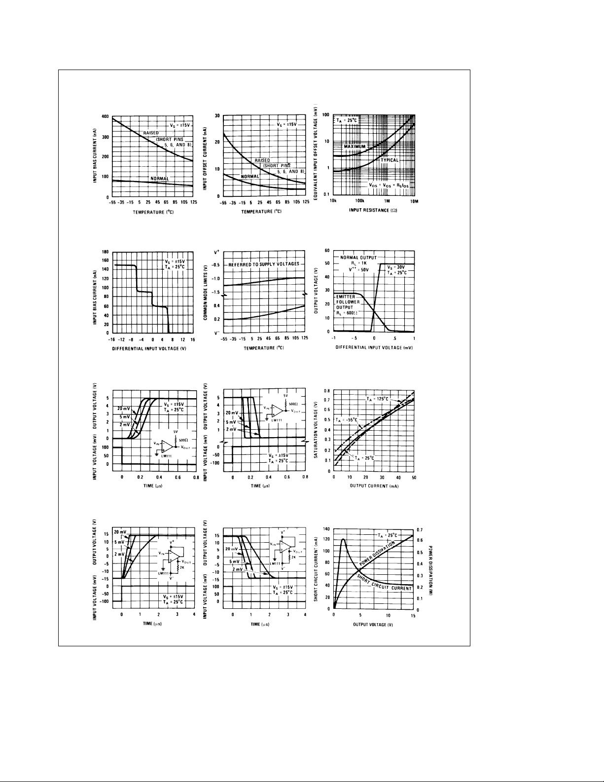
The LM111, LM211 and LM311 are voltage comparators
that have input currents nearly a thousand times lower than
devices like the LM106 or LM710. They are also designed
to operate over a wider range of supply voltages: from stan-
dard
g
15V op amp supplies down to the single 5V supply
used for IC logic. Their output is compatible with RTL, DTL
and TTL as well as MOS circuits. Further, they can drive
lamps or relays, switching voltages up to 50V at currents as
high as 50 mA.
Both the inputs and the outputs of the LM111, LM211 or the
LM311 can be isolated from system ground, and the output
can drive loads referred to ground, the positive supply or the
negative supply. Offset balancing and strobe capability are
provided and outputs can be wire OR’ed. Although slower
than the LM106 and LM710 (200 ns response time vs
40 ns) the devices are also much less prone to spurious
oscillations. The LM111 has the same pin configuration as
the LM106 and LM710.
The LM211 is identical to the LM111, except that its per-
formance is specified over a
b
25
§
Cto
a
85
§
C temperature
range instead of
b
55
§
Cto
a
125
§
C. The LM311 has a tem-
perature range of 0
§
Cto
a
70
§
C.
Features
Y
Operates from single 5V supply
Y
Input current: 150 nA max. over temperature
Y
Offset current: 20 nA max. over temperature
Y
Differential input voltage range:
g
30V
Y
Power consumption: 135 mW at
g
15V
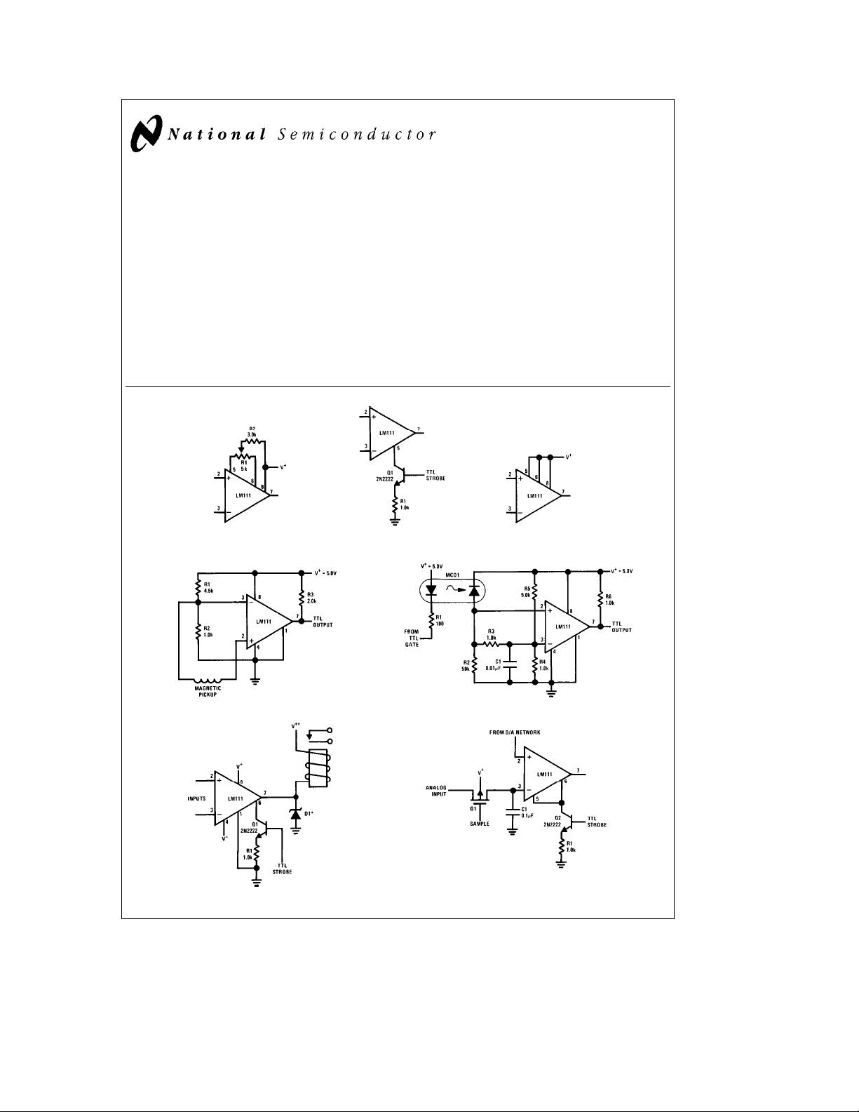
Typical Applications**
**Note: Pin connections shown on schematic di-
agram and typical applications are for
H08 metal can package.
Offset Balancing
Strobing
Note: Do Not
Ground Strobe
Pin. Output is
turned off when
current is pulled
from Strobe Pin.
Increasing Input Stage Current*
*Increases typical common
mode slew from 7.0V/ms
to 18V/ms.
Detector for Magnetic Transducer Digital Transmission Isolator
Relay Driver with Strobe
*Absorbs inductive
kickback of relay and
protects IC from
severe voltage
transients on
V
aa
line.
Note: Do Not Ground Strobe Pin.
Strobing off Both Input* and Output Stages
*Typical input current is
50 pA with inputs strobed off.
Note: Do Not Ground Strobe Pin.
TL/H/5704– 1
C
1995 National Semiconductor Corporation RRD-B30M115/Printed in U. S. A.
Absolute Maximum Ratings for the LM111/LM211
If Military/Aerospace specified devices are required,
please contact the National Semiconductor Sales
Office/Distributors for availability and specifications.
(Note 7)
Total Supply Voltage (V
84
) 36V
Output to Negative Supply Voltage (V
74
) 50V
Ground to Negative Supply Voltage (V
14
) 30V
Differential Input Voltage
g
30V
Input Voltage (Note 1)
g
15V
Output Short Circuit Duration 10 sec
Operating Temperature Range LM111
b
55
§
Cto125
§
C
LM211
b
25
§
Cto85
§
C
Lead Temperature (Soldering, 10 sec) 260
§
C
Voltage at Strobe Pin V
a
b
5V
Soldering Information
Dual-In-Line Package
Soldering (10 seconds)ÀÀÀÀÀÀÀÀÀÀÀÀÀÀÀÀÀÀÀÀÀÀÀ260
§
C
Small Outline Package
Vapor Phase (60 seconds)ÀÀÀÀÀÀÀÀÀÀÀÀÀÀÀÀÀÀÀÀ215
§
C
Infrared (15 seconds) ÀÀÀÀÀÀÀÀÀÀÀÀÀÀÀÀÀÀÀÀÀÀÀÀ220
§
C
See AN-450 ‘‘Surface Mounting Methods and Their Effect
on Product Reliability’’ for other methods of soldering sur-
face mount devices.
ESD Rating (Note 8) 300V
Electrical Characteristics for the LM111 and LM211 (Note 3)
Parameter Conditions Min Typ Max Units
Input Offset Voltage (Note 4) T
A
e
25
§
C, R
S
s
50k 0.7 3.0 mV
Input Offset Current T
A
e
25
§
C 4.0 10 nA
Input Bias Current T
A
e
25
§
C 60 100 nA
Voltage Gain T
A
e
25
§
C 40 200 V/mV
Response Time (Note 5) T
A
e
25
§
C 200 ns
Saturation Voltage V
IN
s
b
5 mV, I
OUT
e
50 mA
0.75 1.5 V
T
A
e
25
§
C
Strobe ON Current (Note 6) T
A
e
25
§
C 2.0 5.0 mA
Output Leakage Current V
IN
t
5 mV, V
OUT
e
35V
0.2 10 nA
T
A
e
25
§
C, I
STROBE
e
3mA
Input Offset Voltage (Note 4) R
S
s
50 k 4.0 mV
Input Offset Current (Note 4) 20 nA
Input Bias Current 150 nA
Input Voltage Range V
a
e
15V, V
b
eb
15V, Pin 7
b
14.5 13.8,-14.7 13.0 V
Pull-Up May Go To 5V
Saturation Voltage V
a
t
4.5V, V
b
e
0
0.23 0.4 V
V
IN
s
b
6 mV, I
OUT
s
8mA
Output Leakage Current V
IN
t
5 mV, V
OUT
e
35V 0.1 0.5 mA
Positive Supply Current T
A
e
25
§
C 5.1 6.0 mA
Negative Supply Current T
A
e
25
§
C 4.1 5.0 mA
Note 1: This rating applies for
g
15 supplies. The positive input voltage limit is 30V above the negative supply. The negative input voltage limit is equal to the
negative supply voltage or 30V below the positive supply, whichever is less.
Note 2: The maximum junction temperature of the LM111 is 150
§
C, while that of the LM211 is 110
§
C. For operating at elevated temperatures, devices in the H08
package must be derated based on a thermal resistance of 165
§
C/W, junction to ambient, or 20
§
C/W, junction to case. The thermal resistance of the dual-in-line
package is 110
§
C/W, junction to ambient.
Note 3: These specifications apply for V
S
e
g
15V and Ground pin at ground, and
b
55
§
C
s
T
A
s
a
125
§
C, unless otherwise stated. With the LM211, however, all
temperature specifications are limited to
b
25
§
C
s
T
A
s
a
85
§
C. The offset voltage, offset current and bias current specifications apply for any supply voltage from a
single 5V supply up to
g
15V supplies.
Note 4: The offset voltages and offset currents given are the maximum values required to drive the output within a volt of either supply witha1mAload. Thus,
these parameters define an error band and take into account the worst-case effects of voltage gain and R
S
.
Note 5: The response time specified (see definitions) is for a 100 mV input step with 5 mV overdrive.
Note 6: This specification gives the range of current which must be drawn from the strobe pin to ensure the output is properly disabled. Do not short the strobe pin
to ground; it should be current driven at 3 to 5 mA.
Note 7: Refer to RETS111X for the LM111H, LM111J and LM111J-8 military specifications.
Note 8: Human body model, 1.5 kX in series with 100 pF.
2
Absolute Maximum Ratings for the LM311
If Military/Aerospace specified devices are required,
please contact the National Semiconductor Sales
Office/Distributors for availability and specifications.
Total Supply Voltage (V
84
) 36V
Output to Negative Supply Voltage V
74
) 40V
Ground to Negative Supply Voltage V
14
) 30V
Differential Input Voltage
g
30V
Input Voltage (Note 1)
g
15V
Power Dissipation (Note 2) 500 mW
ESD Rating (Note 7) 300V
Output Short Circuit Duration 10 sec
Operating Temperature Range 0
§
to 70
§
C
Storage Temperature Range
b
65
§
Cto150
§
C
Lead Temperature (soldering, 10 sec) 260
§
C
Voltage at Strobe Pin V
a
b
5V
Soldering Information
Dual-In-Line Package
Soldering (10 seconds)ÀÀÀÀÀÀÀÀÀÀÀÀÀÀÀÀÀÀÀÀÀÀÀ260
§
C
Small Outline Package
Vapor Phase (60 seconds)ÀÀÀÀÀÀÀÀÀÀÀÀÀÀÀÀÀÀÀÀ215
§
C
Infrared (15 seconds) ÀÀÀÀÀÀÀÀÀÀÀÀÀÀÀÀÀÀÀÀÀÀÀÀ220
§
C
See AN-450 ‘‘Surface Mounting Methods and Their Effect
on Product Reliability’’ for other methods of soldering sur-
face mount devices.
Electrical Characteristics for the LM311 (Note 3)
Parameter Conditions Min Typ Max Units
Input Offset Voltage (Note 4) T
A
e
25
§
C, R
S
s
50k 2.0 7.5 mV
Input Offset Current (Note 4) T
A
e
25
§
C 6.0 50 nA
Input Bias Current T
A
e
25
§
C 100 250 nA
Voltage Gain T
A
e
25
§
C 40 200 V/mV
Response Time (Note 5) T
A
e
25
§
C 200 ns
Saturation Voltage V
IN
s
b
10 mV, I
OUT
e
50 mA
0.75 1.5 V
T
A
e
25
§
C
Strobe ON Current (Note 6) T
A
e
25
§
C 2.0 5.0 mA
Output Leakage Current V
IN
t
10 mV, V
OUT
e
35V
T
A
e
25
§
C, I
STROBE
e
3 mA 0.2 50 nA
V
b
e
Pin 1
eb
5V
Input Offset Voltage (Note 4) R
S
s
50K 10 mV
Input Offset Current (Note 4) 70 nA
Input Bias Current 300 nA
Input Voltage Range
b
14.5 13.8,
b
14.7 13.0 V
Saturation Voltage V
a
t
4.5V, V
b
e
0
0.23 0.4 V
V
IN
s
b
10 mV, I
OUT
s
8mA
Positive Supply Current T
A
e
25
§
C 5.1 7.5 mA
Negative Supply Current T
A
e
25
§
C 4.1 5.0 mA
Note 1: This rating applies for
g
15V supplies. The positive input voltage limit is 30V above the negative supply. The negative input voltage limit is equal to the
negative supply voltage or 30V below the positive supply, whichever is less.
Note 2: The maximum junction temperature of the LM311 is 110
§
C. For operating at elevated temperature, devices in the H08 package must be derated based on a
thermal resistance of 165
§
C/W, junction to ambient, or 20
§
C/W, junction to case. The thermal resistance of the dual-in-line package is 100
§
C/W, junction to
ambient.
Note 3: These specifications apply for V
S
e
g
15V and Pin 1 at ground, and 0
§
C
k
T
A
k
a
70
§
C, unless otherwise specified. The offset voltage, offset current and
bias current specifications apply for any supply voltage from a single 5V supply up to
g
15V supplies.
Note 4: The offset voltages and offset currents given are the maximum values required to drive the output within a volt of either supply with 1 mA load. Thus, these
parameters define an error band and take into account the worst-case effects of voltage gain and R
S
.
Note 5: The response time specified (see definitions) is for a 100 mV input step with 5 mV overdrive.
Note 6: This specification gives the range of current which must be drawn from the strobe pin to ensure the output is properly disabled. Do not short the strobe pin
to ground; it should be current driven at 3 to 5 mA.
Note 7: Human body model, 1.5 kX in series with 100 pF.
3
LM111/LM211 Typical Performance Characteristics
Input Bias Current Input Offset Current Offset Error
Input Characteristics Common Mode Limits Transfer Function
Response Time for Various
Input Overdrives
Response Time for Various
Input Overdrives Output Saturation Voltage
Response Time for Various
Input Overdrives
Response Time for Various
Input Overdrives Output Limiting Characteristics
TL/H/5704– 2
4
剩余18页未读,继续阅读
资源评论
- majiqi0442015-03-06很好的材料,有用
- hsq19912013-05-25有用,帮了大忙,很容易懂.
意欲孤魂
- 粉丝: 1
- 资源: 3
上传资源 快速赚钱
- 我的内容管理 展开
- 我的资源 快来上传第一个资源
- 我的收益 登录查看自己的收益
- 我的积分 登录查看自己的积分
- 我的C币 登录后查看C币余额
- 我的收藏
- 我的下载
- 下载帮助
安全验证
文档复制为VIP权益,开通VIP直接复制
信息提交成功