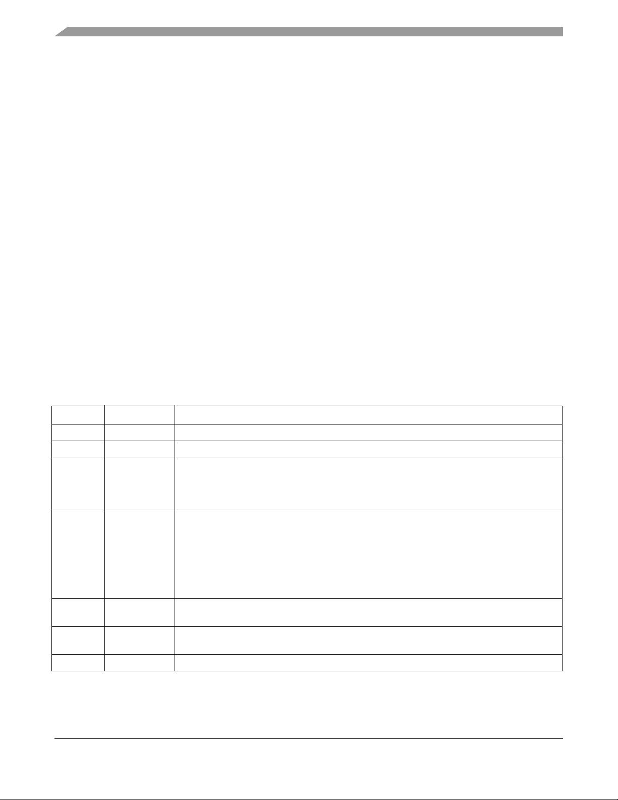
没有合适的资源?快使用搜索试试~ 我知道了~
M9S8LL16C的PDF资料
5星 · 超过95%的资源 需积分: 50 75 下载量 86 浏览量
2013-06-18
17:01:00
上传
评论
收藏 984KB PDF 举报
温馨提示
试读
44页
M9S8LL16C的PDF资料,详细资料M9S8LL16C的PDF资料,下载M9S8LL16C的PDF资料
资源推荐
资源详情
资源评论
64-LQFP
Case 840F
48-LQFP
Case 932
48-QFN
1314
Features
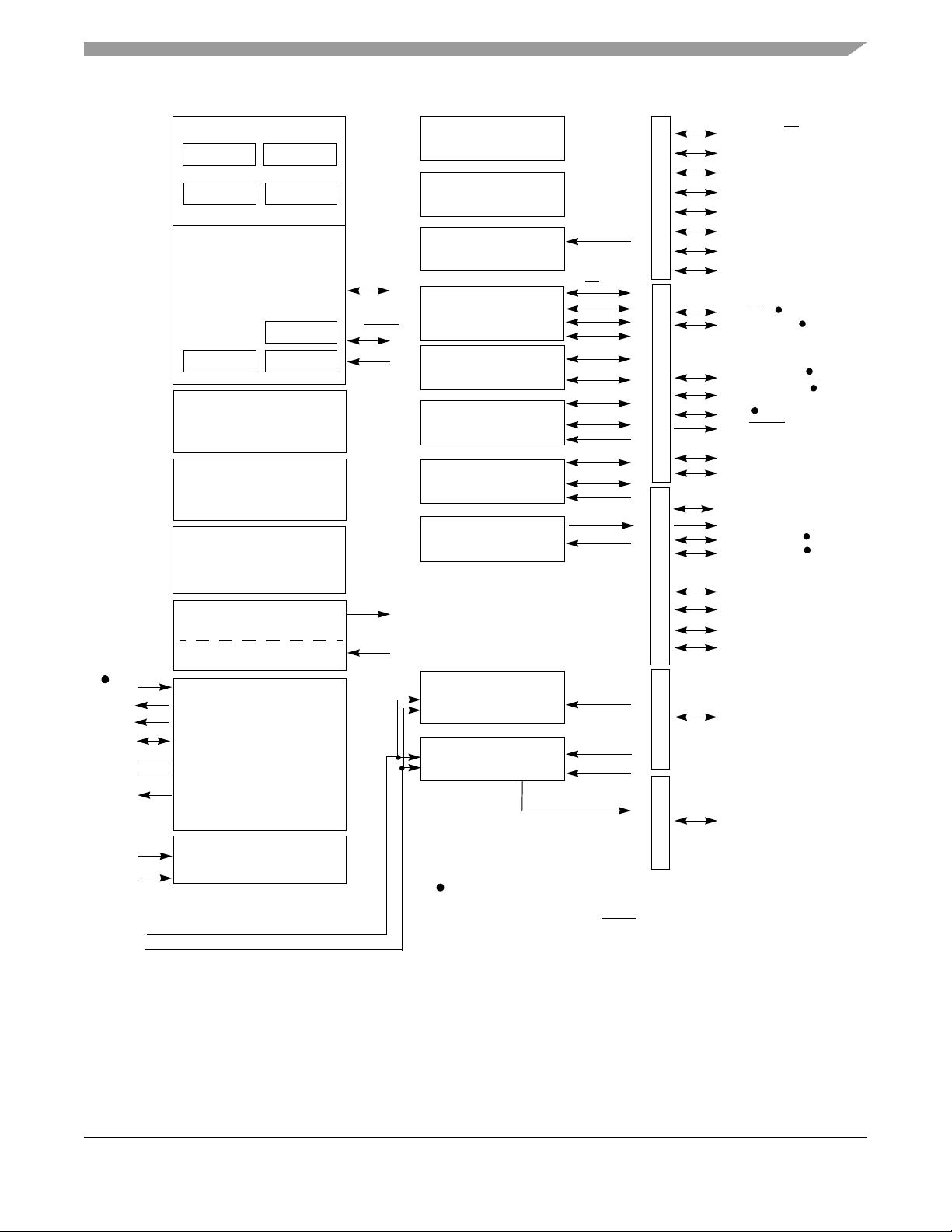
• 8-Bit HCS08 Central Processor Unit (CPU)
– Up to 20-MHz CPU at 3.6V to 1.8V across temperature range
of -40°C to 85°C
– HC08 instruction set with added BGND instruction
– Support for up to 32 interrupt/reset sources
• On-Chip Memory
– Dual Array FLASH read/program/erase over full operating
voltage and temperature
– Random-access memory (RAM)
– Security circuitry to prevent unauthorized access to RAM and
FLASH contents
• Power-Saving Modes
– Two low power stop modes
– Reduced power wait mode
– Low power run and wait modes allow peripherals to run while
voltage regulator is in standby
– Peripheral clock gating register can disable clocks to unused
modules, thereby reducing currents.
– Very low power external oscillator that can be used in stop2 or
stop3 modes to provide accurate clock source to real time
counter
– 6 usec typical wake up time from stop3 mode
• Clock Source Options
– Oscillator (XOSC) — Loop-control Pierce oscillator; Crystal
or ceramic resonator range of 31.25 kHz to 38.4 kHz or 1 MHz
to 16 MHz
– Internal Clock Source (ICS) — Internal clock source module
containing a frequency-locked-loop (FLL) controlled by
internal or external reference; precision trimming of internal
reference allows 0.2% resolution and 2% deviation over
temperature and voltage; supports bus frequencies from 1MHz
to 10 MHz.
• System Protection
– Watchdog computer operating properly (COP) reset with
option to run from dedicated 1-kHz internal clock source or
bus clock
– Low-Voltage Warning with interrupt
– Low-Voltage Detection with reset or interrupt
– Illegal opcode and illegal address detection with reset
– Flash block protection
• Development Support
– Single-wire background debug interface
– Breakpoint capability to allow single breakpoint setting during
in-circuit debugging (plus two more breakpoints in on-chip
debug module)
– On-chip in-circuit emulator (ICE) debug module containing
three comparators and nine trigger modes. Eight deep FIFO for
storing change-of-flow addresses and event-only data. Debug
module supports both tag and force breakpoints
•Peripherals
– LCD — 4x28 or 8x24 LCD driver with internal charge pump
and option to provide an internally regulated LCD reference
that can be trimmed for contrast control.
– ADC — 8-channel, 12-bit resolution; 2.5 μs conversion time;
automatic compare function; temperature sensor; internal
bandgap reference channel; operation in stop3; fully functional
from 3.6V to 1.8V
– ACMP — Analog comparator with selectable interrupt on
rising, falling, or either edge of comparator output; compare
option to fixed internal bandgap reference voltage; outputs can
be optionally routed to TPM module; operation in stop3
– SCI — Full duplex non-return to zero (NRZ); LIN master
extended break generation; LIN slave extended break
detection; wake up on active edge
– SPI— Full-duplex or single-wire bidirectional;
Double-buffered transmit and receive; Master or Slave mode;
MSB-first or LSB-first shifting
– IIC — IIC with up to 100 kbps with maximum bus loading;
Multi-master operation; Programmable slave address;
Interrupt driven byte-by-byte data transfer; supports broadcast
mode and 10-bit addressing
– TPMx — Two 2-channel (TPM1 and TPM2); Selectable input
capture, output compare, or buffered edge- or center-aligned
PWM on each channel;
– TOD— (Time Of Day) 8-bit quarter second counter with
match register; External clock source for precise time base,
time-of-day, calendar or task scheduling functions; Free
running on-chip low power oscillator (1 kHz) for cyclic
wake-up without external components.
• Input/Output
– 38 GPIOs, 2 output-only pins
– 8 KBI interrupts with selectable polarity
– Hysteresis and configurable pull up device on all input pins;
Configurable slew rate and drive strength on all output pins.
• Package Options
– 64-LQFP, 48-LQFP and 48-QFN
Freescale Semiconductor
Data Sheet: Technical Data
An Energy Efficient Solution by Freescale
Document Number: MC9S08LL16
Rev. 7, 1/2013
MC9S08LL16 Series
Covers: MC9S08LL16 and
MC9S08LL8
MC9S08LL16 Series MCU Data Sheet, Rev. 7
Freescale Semiconductor2
Revision History
To provide the most up-to-date information, the revision of our documents on the World Wide Web will
be the most current. Your printed copy may be an earlier revision. To verify you have the latest information
available, refer to:
http://freescale.com/
The following revision history table summarizes changes contained in this document.
Rev Date Description of Changes
1 9/2008 Initial Release.
2 10/2008 Updated electrical characteristics.
3 01/2009
Corrected 48-Pin QFN/LQFP pinouts for pins 29, 30, 32, and 32 in Figure 3.
Extracted Stop Mode Adders from the Supply Current table and created a Separate
table for the data (See Table 1 0 ). Added missing power consumption parameters in
Supply Current Characteristics (Ta bl e 9 ).
4 07/21/2009
Completed all the TBDs.
Changed V
DDAD
to V
DDA
, V
SSAD
to V
SSA
, I
DDAD
to I
DDA.
Corrected the data in the Table 8, and added
|I
InT
|. Completed the Figure in the
Section 3.6, “DC Characteristics.”
Corrected RI
DD
in FEI mode with all modules on, WI
DD
at 8 MHz, FEI mode with all
modules off, S2I
DD
, S3I
DD
; added ApS3I
DD
in the Table 9.
Corrected E
TUE
, DNL, INL, E
ZS
, E
FS
, E
Q
, and E
IL
in the Table 18.
5 10/13/2009
Updated R
PU
/R
PD
data in the Ta ble 8 .
Added Figure 5.
6 10/27/2010
Changed the Max. of R
PU
/R
PD
at PTA[4:5], PTD[0:77] and PTE[0:7] to 69.5
kΩ
in the
Ta b l e 8.
7 1/23/2013 Updated
|I
In
| in the
Ta b l e 8.
1 Devices in the MC9S08LL16 Series . . . . . . . . . . . . . . 4
2 Pin Assignments . . . . . . . . . . . . . . . . . . . . . . . . . . . . . 6
3 Electrical Characteristics . . . . . . . . . . . . . . . . . . . . . . . 9
3.1 Introduction . . . . . . . . . . . . . . . . . . . . . . . . . . . . . 9
3.2 Parameter Classification . . . . . . . . . . . . . . . . . . . 9
3.3 Absolute Maximum Ratings. . . . . . . . . . . . . . . . 10
3.4 Thermal Characteristics. . . . . . . . . . . . . . . . . . . 11
3.5 ESD Protection and Latch-Up Immunity . . . . . . 12
3.6 DC Characteristics. . . . . . . . . . . . . . . . . . . . . . . 13
3.7 Supply Current Characteristics . . . . . . . . . . . . . 25
3.8 External Oscillator (XOSCVLP) Characteristics 27
3.9 Internal Clock Source (ICS) Characteristics . . . 28
3.10 AC Characteristics . . . . . . . . . . . . . . . . . . . . . . .30
3.10.1Control Timing. . . . . . . . . . . . . . . . . . . . . .30
3.10.2TPM Module Timing . . . . . . . . . . . . . . . . .31
3.10.3SPI Timing . . . . . . . . . . . . . . . . . . . . . . . .32
3.11 Analog Comparator (ACMP) Electricals . . . . . . .35
3.12 ADC Characteristics . . . . . . . . . . . . . . . . . . . . . .35
3.13 LCD Specifications . . . . . . . . . . . . . . . . . . . . . . .39
3.14 Flash Specifications . . . . . . . . . . . . . . . . . . . . . .39
3.15 EMC Performance . . . . . . . . . . . . . . . . . . . . . . .40
3.15.1Radiated Emissions . . . . . . . . . . . . . . . . .40
4 Ordering Information . . . . . . . . . . . . . . . . . . . . . . . . . .41
4.1 Device Numbering System . . . . . . . . . . . . . . . . .41
Table of Contents
MC9S08LL16 Series MCU Data Sheet, Rev. 7
Freescale Semiconductor 3
Related Documentation
Find the most current versions of all documents at: http://www.freescale.com
Reference Manual (MC9S08LL16RM)
Contains extensive product information including modes of operation, memory,
resets and interrupts, register definition, port pins, CPU, and all module
information.
MC9S08LL16 Series MCU Data Sheet, Rev. 7
Devices in the MC9S08LL16 Series
Freescale Semiconductor4
1 Devices in the MC9S08LL16 Series
Table 1
summarizes the feature set available in the MC9S08LL16 series of MCUs.
t
The block diagram in Figure 1 shows the structure of the MC9S08LL16 series MCU.
Table 1. MC9S08LL16 Series Features by MCU and Package
Feature MC9S08LL16 MC9S08LL8
Package
64-pin
LQFP
48-pin
QFN/LQFP
48-pin
QFN/LQFP
FLASH
16,384
(Dual 8K Arrays)
10,240
(8K and 2K
arrays)
RAM 2080 2080 2080
ACMP yes yes yes
ADC 8-ch 8-ch 8-ch
IIC yes yes yes
IRQ yes yes yes
KBI 8 8 8
SCI yes yes yes
SPI yes yes yes
TPM1 2-ch 2-ch 2-ch
TPM2 2-ch - -
TOD Yes Yes Yes
LCD
8x24
4x28
8x16
4x20
8x16
4x20
I/O pins
1
1
I/O does not include two output-only port pins.
38 31 31
Devices in the MC9S08LL16 Series
MC9S08LL16 Series MCU Data Sheet, Rev. 7
Freescale Semiconductor 5
Figure 1. MC9S08LL16 Series Block Diagram
8-BIT KEYBOARD
INTERRUPT (KBI)
IIC MODULE (IIC)
SERIAL PERIPHERAL
INTERFACE (SPI)
USER FLASH B
USER RAM
ON-CHIP ICE
DEBUG MODULE (DBG)
(LL16 = 8K BYTES)
HCS08 CORE
CPU
BKGD
INT
BKP
2-CHANNEL TIMER/PWM
(TPM1)
HCS08 SYSTEM CONTROL
RESETS AND INTERRUPTS
MODES OF OPERATION
POWER MANAGEMENT
COP
IRQ LVD
LOW-POWER OSCILLATOR
INTERNAL CLOCK
Source (ICS)
SERIAL COMMUNICATIONS
2-CHANNEL TIMER/PWM
(TPM2)
(LL8 = 2K BYTES)
V
LL1
V
LCD
LCD
V
LL2
V
LL3
V
CAP1
V
CAP2
LCD[31:0]
V
SS
V
DD
VOLTAGE
REGULATOR
USER FLASH A
(LL8 = 8K BYTES)
PTC7/IRQ/TCLK
PTC5/TPM2CH1
PTC4/TPM2CH0
PTC3/TPM1CH1
PORT B
PTB5/MOSI/SCL
PTB4/MISO/SDA
PTB3
PTB2/RESET
PTB1/XTAL
PTB0/EXTAL
PTA7/KBIP7/ADP7/ACMP–
PTA6/KBIP6/ADP6/ACMP+
PTA4/KBIP4/ADP4/LCD30
INTERFACE (SCI)
PTB7/SS
PTB6/SPSCK
PTC1/TxD
PTC0/RxD
TxD
RxD
SS
SPSCK
SCL
SDA
MOSI
MISO
V
SSA
/V
REFL
V
DDA
/V
REFH
XTAL
EXTAL
IRQ
KBI[7:0]
PORT A
RESET
TPM2CH0
LIQUID CRYSTAL
DISPLAY DRIVER
ANALOG-TO-DIGITAL
CONVERTER (ADC)
12-BIT
ANALOG COMPARATOR
(ACMP)
ACMP+
ACMP–
AD[7:0]
TIME OF DAY MODULE
(TOD)
TPM2CH1
TCLK
TPM1CH0
TPM1CH1
TCLK
PTA1/KBIP1/SPSCK/ADP1
PORT C
PORT D
PORT E
PTD[7:0]/LCD[7:0]
PTE[7:0]/LCD[15:8]
PTC6/ACMPO//BKGD/MS
PTC2/TPM1CH0
Pins not available on 48-pin packages.
Notes:
When PTB2 is configured as RESET, pin becomes bi-directional with
output being open-drain drive containing an internal pull-up device.
(LL16 = 8K BYTES)
(LL8 = 2K BYTES)
(LL16 = 2K BYTES)
PTA5/KBIP5/ADP5/LCD31
LCD[23:16] not available on 48-pin packages.
ACMPO
BKGD/MS
When PTC6 is configured as BKGD, pin becomes bi-directional.
K
EY
:
PTA0/KBIP0/SS/ADP0
PTA2/KBIP2/SDA/MISO/ADP2
PTA3/KBIP3/SCL/MOSI/ADP3
剩余43页未读,继续阅读
资源评论
- 南京搬运工2016-03-18有借鉴价值,这个PDF不应该花费我的积分呀
- Q233282002017-10-07血糖仪里用的
- ly_ring2013-07-30使用飞思卡尔mc9s08ll16c,可是芯片上是m9s8ll16c,假的? 下载pdf也没找到mark
- jyrpxj2018-04-04使用飞思卡尔mc9s08ll16c...
- harder5212014-06-17使用飞思卡尔mc9s08ll16c
chanjan01
- 粉丝: 0
- 资源: 6
上传资源 快速赚钱
- 我的内容管理 展开
- 我的资源 快来上传第一个资源
- 我的收益 登录查看自己的收益
- 我的积分 登录查看自己的积分
- 我的C币 登录后查看C币余额
- 我的收藏
- 我的下载
- 下载帮助
安全验证
文档复制为VIP权益,开通VIP直接复制
信息提交成功