5
5
4
4
3
3
2
2
1
1
D D
C C
B B
A A
P_ON
power12V
AV2
AV1
power12V
AV2
AV1 YIN
VCM
CVBSIN
DGND
DGND
DGND
DGND
DGND
D+5V
DGNDDGND
DGND DGND DGND
AGND
DGND
DGND
A
AGND
A
AGND
D
DGND
D+5V
D
DGND
D+3.3V D+5V
D
DGND
D
DGND
D+1.8V
D
DGND
D
DGND
D
DGND
D
DGND
DGND
A
AGND
YIN 2
VCM 2
CVBSIN 2AV22
Title
Size Document Number Rev
Date: Sheet of
Fax
:
::
:
886-2-2778-1050
Tel
:
::
:
886-2-2778-5939
5F,No.136, Sec.3, Nanjing E. Road,Taipei,Taiwan,R.O.C.
Beyond Innovation Technology Co., LTD.
Task Code
The circuits shown are intended to explain typical application of the products concerned.
BiTEK is not responsible for any infringement of third party or any other intellectual property
rights that may arise from the use of these circuits.
1.00
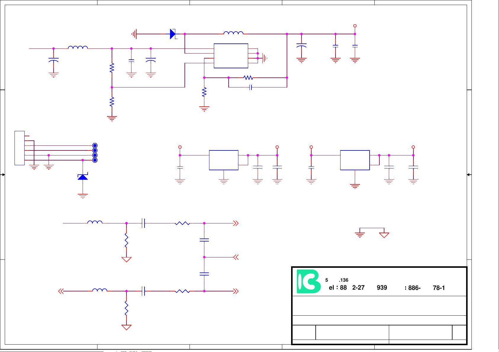
01. POWER
A
1 4Friday, September 13, 2013
TP2TP2
C14 1uFC14 1uF
C16
47pF
C16
47pF
C4
100UF/35V
C4
100UF/35V
R8
75R
R8
75R
C1
470UF/10V
C1
470UF/10V
C8
0.1uF
C8
0.1uF
TP3TP3
C9
10uF
C9
10uF
R2 11K/1%R2 11K/1%
TP4TP4
C6
100UF/35V
C6
100UF/35V
R5 56RR5 56R
C10
0.1uF
C10
0.1uF
C11
0.1uF
C11
0.1uF
C12
10uF
C12
10uF
L4 1.5uHL4 1.5uH
C15
47pF
C15
47pF
R6
75R
R6
75R
D1
SS14
D1
SS14
1 2
U1 TD1509U1 TD1509
VIN
1
OUT
2
FB
3
ON/OFF
4
GND
5
GND
6
GND
7
GND
8
L2 47uHL2 47uH
R1
NC
R1
NC
C3
10uF/16V
C3
10uF/16V
D2
SS14
D2
SS14
1 2
U2 BIT1117-3.3VU2 BIT1117-3.3V
GND
1
OUT
2
IN
3
OUT
4
C13
0.1uF
C13
0.1uF
C5
0.1uF
C5
0.1uF
C17 1uFC17 1uF
C2
0.1uF
C2
0.1uF
C7 10nFC7 10nF
R3
3.6K/1%
R3
3.6K/1%
R7 56RR7 56R
TP1TP1
JP1
6P2.0
JP1
6P2.0
1
2
3
4
5
6
L3 1.5uHL3 1.5uH
R4
0R
R4
0R
U3 BIT1117-1.8VU3 BIT1117-1.8V
GND
1
OUT
2
IN
3
OUT
4
L1 47uHL1 47uH


