没有合适的资源?快使用搜索试试~ 我知道了~
温馨提示
试读
72页
Over the past five years, the development of true analog CMOS processes has led to the use of high-speed analog devices in the digital arena. System speeds of 150 MHz and higher have become common for digital logic. Systems that were considered high end and high speed a few years ago are now cheaply and easily implemented. However, this integration of fast system speeds brings with it the challenges of analog system design to a digital world. This document is a guideline for printed circuit board (PCB) layouts and designs associated with high-speed systems.
资源推荐
资源详情
资源评论
Altera Corporation 1
AN-315-1.1 Preliminary
Application Note
Guidelines for Designing
High-Speed FPGA PCBs
Introduction
Over the past five years, the development of true analog CMOS processes
has led to the use of high-speed analog devices in the digital arena.
System speeds of 150 MHz and higher have become common for digital
logic. Systems that were considered high end and high speed a few years
ago are now cheaply and easily implemented. However, this integration
of fast system speeds brings with it the challenges of analog system
design to a digital world. This document is a guideline for printed circuit
board (PCB) layouts and designs associated with high-speed systems.
“High speed” does not just mean faster communication rates (e.g., faster
than 1 gigabit per second (Gbps)). A transistor-transistor logic (TTL)
signal with a 600-ps rise time is also considered a high-speed signal. This
opens up the entire PCB to careful and targeted board simulation and
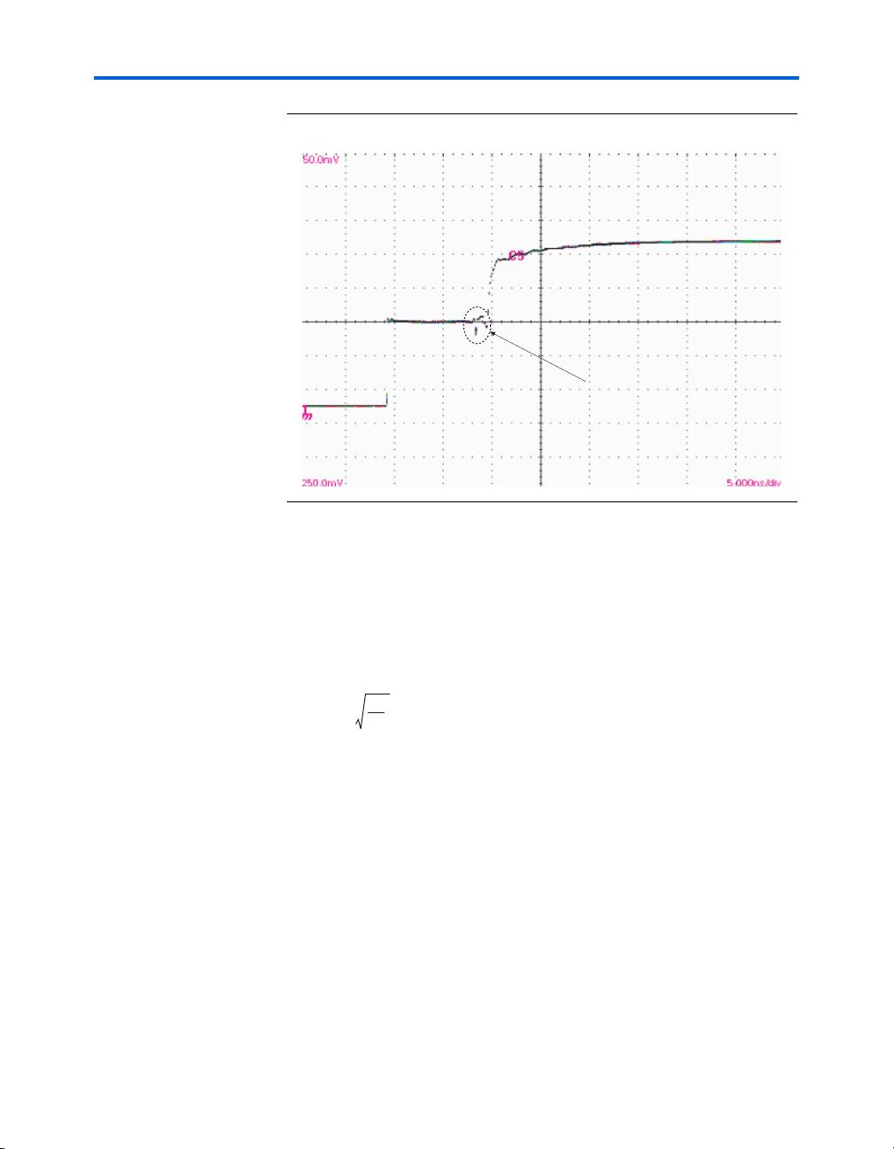
design. The designer must consider any discontinuities on the board. The
“Time-Domain Reflectometry” and “Discontinuity” sections explain how
to eliminate discontinuities on a PCB. Some sources of discontinuities are
vias, right angled bends, and passive connectors.
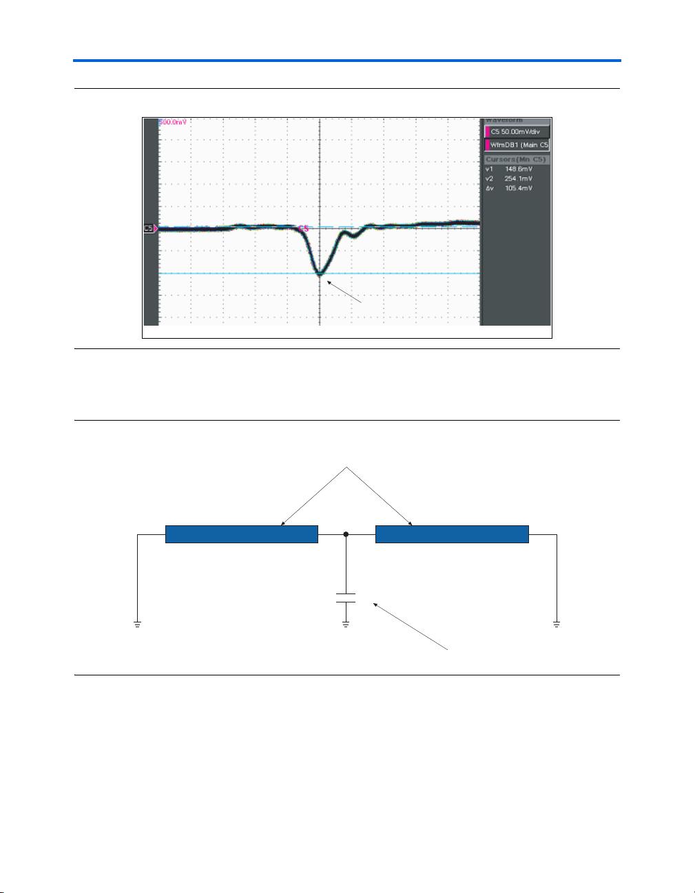
The “Termination” section explains about terminations for signals on
PCBs. The placement and selection of termination resistors are critical in
order to avoid reflections.
As systems require higher speeds, they use differential signals instead of
single-ended signals because of better noise margins and immunity.
Differential signals require special attention from PCB designers with
regards to trace layout. The “Trace Layout” section addresses differential
traces in terms of trace layout. Crosstalk, which can adversely affect
single ended and differential signals alike, is also addressed in this
section.
All the dense, high-speed switching (i.e., hundreds of I/O pins switching
at rates faster than 500-ps rise and fall times) produces powerful transient
changes in power supply voltage. These transient changes occur because
a signal switching at higher frequency consumes a proportionally greater
amount of power than a signal switching at a lower frequency. As a
result, a device does not have a stable power reference that both analog
and digital circuits can derive their power from. This phenomenon is
called simultaneous switching noise (SSN). The “Dielectric Material”
section discusses how to eliminate some of these SSN problems through
careful board design.
February 2004, ver. 1.1
2 Altera Corporation
Preliminary
Guidelines for Designing High-Speed FPGA PCBs Time-Domain Reflectometry
The “Simultaneous Switching Noise” and “Decoupling” sections cover
power supply decoupling and PCB layer stackup. The document
discusses how to select the method and amount of decoupling as well as
the theory behind capacitive decoupling. These sections also present a
real life example of troubleshooting a decoupling problem. The “Layer
Stackup” section discusses layer stackup.
It is critical to follow the best practices described in this document to
ensure the best performance from your system. The content of this
document is based on the results of Altera's experiments with high-speed
PCBs. The simulations were done with Hspice, an analog circuit
simulator. Ansoft 2D and 3D field solvers were used to extract RLGC
parameters for different structures. Sigrity Speed2000 tool was used for
SSN simulation.
This document should be used in conjunction with the board layout
example provided on the Altera web site (www.altera.com). You can also
contact Altera Applications for this example. The board layout example
is a set of specific guidelines used when designing the Stratix GX
development kit board. It includes schematics, a board specific layout
guideline, and board layout and stackup information.
You should also use the characterization report for the Altera FPGA you
are designing for with this document. This document will assist with
design guidelines required for the board design, and the characterization
report will give a picture of the device performance.
Contact Altera Applications for further assistance or questions with
regards to this document or any other issues associated with high-speed
board design.
Time-Domain
Reflectometry
Time domain reflectometry (TDR) is a way to observe discontinuities on
a transmission path. The time domain reflectometer sends a pulse
through the transmission medium. Reflections occur when the pulse of
energy reaches either the end of the transmission path or a discontinuity
within the transmission path. From these reflections, the designer can
determine the size and location of the discontinuity. Many examples in
this handbook use TDR, and this section provides an understanding of
TDR.
Figure 1 shows a TDR voltage plot for a cable that is not connected to a
PCB. The middle line is a 50-Ω cable one meter long. At Point A, a pulse
starts (Z
o
= 50 Ω) and transmits through the cable, stopping at the end of
the transmission line (i.e., Point B). Because the end of the transmission
line is open, there is infinite impedance, Z
LOAD
= α. Therefore, the
reflection coefficient at the load is determined with the equation:
Altera Corporation 3
Preliminary
Time-Domain Reflectometry Guidelines for Designing High-Speed FPGA PCBs
Reflection coefficient = (Z
LOAD
– Z
o
)/(Z
LOAD
+ Z
o
)
Reflection coefficient in this case = (α – 50)/(α + 50) = 1
The entire signal is reflected. At Point B, the amplitude of the signal
doubles. See Figure 1.
Figure 1. TDR Voltage Plot with Cable Not Connected to PCB
If the same meter-long cable is then connected to a PCB through an SMA
connector, the plot changes. See Figure 2. Because the SMA connector is
more capacitive than inductive in nature, it appears as a capacitive load,
shown as a dip in the TDR plot.
50 Ω
Cable
Point B
Point A
4 Altera Corporation
Preliminary
Guidelines for Designing High-Speed FPGA PCBs Time-Domain Reflectometry
Figure 2. TDR Voltage Plot with Cable Connected to PCB
Figure 3 shows an expanded curve for the SMA connector. Because the
rise time of the pulse sent for TDR analysis is very small (around 20 ps),
the TDR voltage plot shows every discontinuity on the transmission path.
The SMA is a capacitive discontinuity on the transmission path, so the
signal dips on the voltage plot. The impedance of an ideal transmission
line is defined by the equation:
Therefore, when the capacitance increases, the impedance decreases. If
the discontinuity is inductive, then the impedance will increase, which
appears as a bump in the TDR plot. You can calculate the capacitance and
inductance from the curves on a TDR plot. If the plot shows a dip, as in
Figure 3, then calculate the capacitance.
Section added due
to the board trace
and connectors
Z
O
=
L
C
Altera Corporation 5
Preliminary
Time-Domain Reflectometry Guidelines for Designing High-Speed FPGA PCBs
Figure 3. TDR Voltage Plot for the Section Around the SMA Connector on PCB
The equivalent circuit approximation for a dip in the TDR plot is a
capacitor to ground, as shown in Figure 4.
Figure 4. Equivalent Circuit for a Transmission Line with Capacitive Discontinuity
The RC equation for this type of circuit is:
R = Z
o
/2
RC = Z
o
C/2
The two transmission lines behave as if they are parallel to each other.
Dip due to the
dominating
capacitance of
the SMA
C
Z
0
Z
0
Transmission Line
Capacitive
Discontinuity
剩余71页未读,继续阅读
资源评论
bigbibby
- 粉丝: 0
- 资源: 4
上传资源 快速赚钱
- 我的内容管理 展开
- 我的资源 快来上传第一个资源
- 我的收益 登录查看自己的收益
- 我的积分 登录查看自己的积分
- 我的C币 登录后查看C币余额
- 我的收藏
- 我的下载
- 下载帮助
安全验证
文档复制为VIP权益,开通VIP直接复制
信息提交成功