


ZC706 Evaluation Board
for the Zynq-7000
XC7Z045 SoC
User Guide
UG954 (v1.8) August 6, 2019
ZC706 Evaluation Board User Guide www.xilinx.com 2
UG954 (v1.8) August 6, 2019
Notice of Disclaimer
The information disclosed to you hereunder (the “Materials”) is provided solely for the selection and use of Xilinx products. To the maximum
extent permitted by applicable law: (1) Materials are made available "AS IS" and with all faults, Xilinx hereby DISCLAIMS ALL WARRANTIES
AND CONDITIONS, EXPRESS, IMPLIED, OR STATUTORY, INCLUDING BUT NOT LIMITED TO WARRANTIES OF MERCHANTABILITY,
NON-INFRINGEMENT, OR FITNESS FOR ANY PARTICULAR PURPOSE; and (2) Xilinx shall not be liable (whether in contract or tort, including
negligence, or under any other theory of liability) for any loss or damage of any kind or nature related to, arising under, or in connection with,
the Materials (including your use of the Materials), including for any direct, indirect, special, incidental, or consequential loss or damage
(including loss of data, profits, goodwill, or any type of loss or damage suffered as a result of any action brought by a third party) even if such
damage or loss was reasonably foreseeable or Xilinx had been advised of the possibility of the same. Xilinx assumes no obligation to correct
any errors contained in the Materials or to notify you of updates to the Materials or to product specifications. You may not reproduce,
modify, distribute, or publicly display the Materials without prior written consent. Certain products are subject to the terms and conditions
of Xilinx’s limited warranty, please refer to Xilinx’s Terms of Sale which can be viewed at www.xilinx.com/legal.htm#tos; IP cores may be
subject to warranty and support terms contained in a license issued to you by Xilinx. Xilinx products are not designed or intended to be
fail-safe or for use in any application requiring fail-safe performance; you assume sole risk and liability for use of Xilinx products in such
critical applications, please refer to Xilinx’s Terms of Sale which can be viewed at www.xilinx.com/legal.htm#tos.
AUTOMOTIVE APPLICATIONS DISCLAIMER
AUTOMOTIVE PRODUCTS (IDENTIFIED AS “XA” IN THE PART NUMBER) ARE NOT WARRANTED FOR USE IN THE DEPLOYMENT OF AIRBAGS
OR FOR USE IN APPLICATIONS THAT AFFECT CONTROL OF A VEHICLE (“SAFETY APPLICATION”) UNLESS THERE IS A SAFETY CONCEPT OR
REDUNDANCY FEATURE CONSISTENT WITH THE ISO 26262 AUTOMOTIVE SAFETY STANDARD (“SAFETY DESIGN”). CUSTOMER SHALL, PRIOR
TO USING OR DISTRIBUTING ANY SYSTEMS THAT INCORPORATE PRODUCTS, THOROUGHLY TEST SUCH SYSTEMS FOR SAFETY PURPOSES.
USE OF PRODUCTS IN A SAFETY APPLICATION WITHOUT A SAFETY DESIGN IS FULLY AT THE RISK OF CUSTOMER, SUBJECT ONLY TO
APPLICABLE LAWS AND REGULATIONS GOVERNING LIMITATIONS ON PRODUCT LIABILITY.
© Copyright 2012–2019 Xilinx, Inc. Xilinx, the Xilinx logo, Artix, ISE, Kintex, Spartan, Virtex, Vivado, Zynq, and other designated brands
included herein are trademarks of Xilinx in the United States and other countries. All other trademarks are the property of their respective
owners.
Revision History
The following table shows the revision history for this document.
Date Version Revision
10/08/2012 1.0
Initial Xilinx release.
11/21/2012 1.1
Added additional user LED in ZC706 Evaluation Board Features section, Table 1-1,
User I/O section, Figure 1-26, and Table 1-28. In Table 1-1, added fan sink
information and updated notes for 10/100/1000 Ethernet PHY, user pushbuttons,
user DIP switch, and FPGA PROG pushbutton. Added Encryption Key Backup Circuit
section. Updated second paragraph in DDR3 SODIMM Memory (PL) section.
Updated second paragraph in SD Card Interface section. Updated Table 1-11.
Added U53 information to first paragraph in HDMI Video Output section. Added
fourth bullet to Real Time Clock (RTC) section. Updated Figure 1-24. Added pin A17
to Table 1-28. Updated Figure 1-33. Replaced UCF in Appendix C. Added additional
reference to Additional Resources.
Send Feedback
ZC706 Evaluation Board User Guide www.xilinx.com 3
UG954 (v1.8) August 6, 2019
04/24/2013 1.2
Chapter 1, ZC706 Evaluation Board Features: Table 1-1 feature descriptions are now
linked to their respective sections in the book. Figure 1-3, Figure 1-34, and
Figure 1-35 were replaced. Table 1-2 was removed because it was a duplicate of
Table 1-11. Table 1-2: Switch SW11 Configuration Option Settings was added. FMC
Connector JTAG Bypass, page 35 was updated. Default lane size information below
Figure 1-18 was changed. Figure 1-19 PCI Express Lane Size Select Jumper J19 was
added. The names of pins 18 and 19 changed in Table 1-17. The address of I
2
C bus
PMBUS_DATA/CLOCK changed in Table 1-25. Reference designator DS35 was added
to Table 1-27. Callout numbers in the User I/O, page 59 section are now linked to
Table 1-1. SW13 information was added to the section User Pushbuttons, page 61.
In Table 1-33, J5 pin H22 changed to XC7Z045 (U1) pin AH26 and H23 changed to
AH27. The section ZC706 Board Power System, page 74 was added. Voltage levels
were changed in VADJ Voltage Control, page 81. Table 1-37 was modified and
Table 1-38 was added.
Appendix A, Default Switch and Jumper Settings: The SW11 selection in Table A-1
changed.
Appendix F, Regulatory and Compliance Information: A link to the master answer
record was added.
07/31/2013 1.3
Updated Table 1-22. Replaced the master User Constraints File (UCF) list in
Appendix C, Xilinx Constraints File with the master Xilinx Design Constraints (XDC)
list. Updated references throughout the document.
04/28/2015 1.4
Updated “LMZ22000 Family Regulator Description” to LMZ31500 and LMZ31700
Family Regulator Description. Updated Table 1-4, Table 1-7, Table 1-13, Table 1-23,
Table 1-28 through Table 1-30, Table 1-32 through Table 1-34, Table 1-36, and
Table A-2. Added Figure A-1. Updated Appendix C, Xilinx Constraints File.
09/10/2015 1.5
Updated J48 header jumper setting (third row in Table 1-7).
03/29/2016 1.6
Updated value of C6 in Figure 1-33 from 270 pF to 5600 pF.
07/01/2018 1.7
Editorial updates only. No technical content updates.
08/06/2019 1.8
Updated Figure 1-27 from VADJ to VCC1V5_PL. Appendix F, Regulatory and
Compliance Information: An updated link to the master answer record was added.
Date Version Revision
Send Feedback
ZC706 Evaluation Board User Guide www.xilinx.com 4
UG954 (v1.8) August 6, 2019
Table of Contents
Revision History . . . . . . . . . . . . . . . . . . . . . . . . . . . . . . . . . . . . . . . . . . . . . . . . . . . . . . . . . . . . . . . . . . . . 2
Chapter 1: ZC706 Evaluation Board Features
Overview . . . . . . . . . . . . . . . . . . . . . . . . . . . . . . . . . . . . . . . . . . . . . . . . . . . . . . . . . . . . . . . . . . . . . . . . 7
ZC706 Evaluation Board Features . . . . . . . . . . . . . . . . . . . . . . . . . . . . . . . . . . . . . . . . . . . . . . . . . . . . . . . . . . . . .7
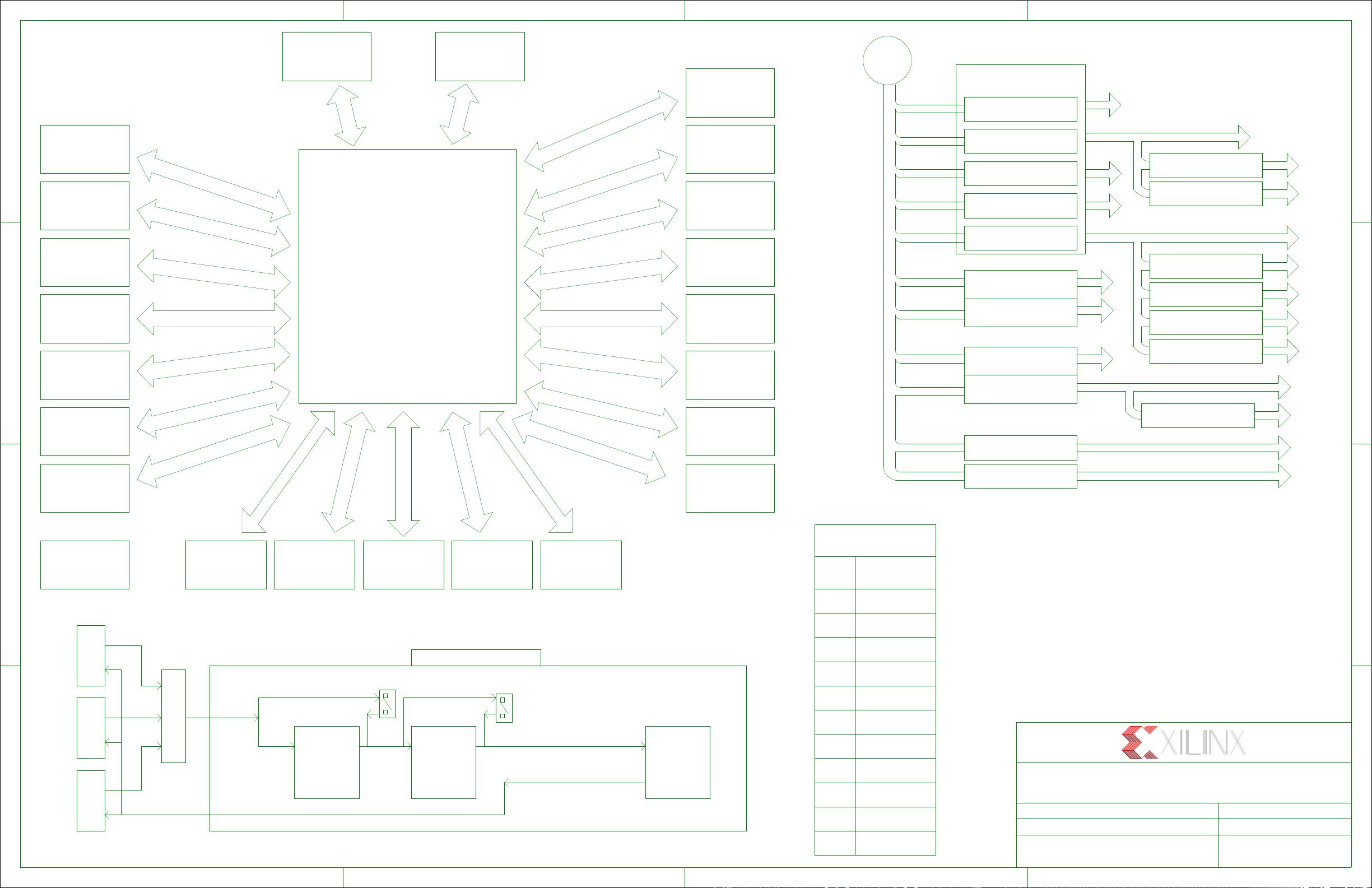
Block Diagram . . . . . . . . . . . . . . . . . . . . . . . . . . . . . . . . . . . . . . . . . . . . . . . . . . . . . . . . . . . . . . . . . . . . . . . . . . . .10
Board Layout . . . . . . . . . . . . . . . . . . . . . . . . . . . . . . . . . . . . . . . . . . . . . . . . . . . . . . . . . . . . . . . . . . . . . . . . . . . . .10
Discharge Caution . . . . . . . . . . . . . . . . . . . . . . . . . . . . . . . . . . . . . . . . . . . . . . . . . . . . . . . . . . . . . . . . 11
Feature Descriptions . . . . . . . . . . . . . . . . . . . . . . . . . . . . . . . . . . . . . . . . . . . . . . . . . . . . . . . . . . . . . . 15
Zynq-7000 XC7Z045 SoC . . . . . . . . . . . . . . . . . . . . . . . . . . . . . . . . . . . . . . . . . . . . . . . . . . . . . . . . . . . . . . . . . . . .15
Device Configuration . . . . . . . . . . . . . . . . . . . . . . . . . . . . . . . . . . . . . . . . . . . . . . . . . . . . . . . . . . . . . . . . . . . . . . . . . . . . . 16
Encryption Key Backup Circuit . . . . . . . . . . . . . . . . . . . . . . . . . . . . . . . . . . . . . . . . . . . . . . . . . . . . . . . . . . . . . . . . . . . . .17
I/O Voltage Rails . . . . . . . . . . . . . . . . . . . . . . . . . . . . . . . . . . . . . . . . . . . . . . . . . . . . . . . . . . . . . . . . . . . . . . . . . . . . . . . . . 18
DDR3 SODIMM Memory (PL) . . . . . . . . . . . . . . . . . . . . . . . . . . . . . . . . . . . . . . . . . . . . . . . . . . . . . . . . . . . . . . . .19
DDR3 Component Memory (PS) . . . . . . . . . . . . . . . . . . . . . . . . . . . . . . . . . . . . . . . . . . . . . . . . . . . . . . . . . . . . . .23
Quad-SPI Flash Memory . . . . . . . . . . . . . . . . . . . . . . . . . . . . . . . . . . . . . . . . . . . . . . . . . . . . . . . . . . . . . . . . . . . .26
USB 2.0 ULPI Transceiver . . . . . . . . . . . . . . . . . . . . . . . . . . . . . . . . . . . . . . . . . . . . . . . . . . . . . . . . . . . . . . . . . . .29
SD Card Interface . . . . . . . . . . . . . . . . . . . . . . . . . . . . . . . . . . . . . . . . . . . . . . . . . . . . . . . . . . . . . . . . . . . . . . . . . .31
Programmable Logic JTAG Programming Options . . . . . . . . . . . . . . . . . . . . . . . . . . . . . . . . . . . . . . . . . . . . . . .33
Programmable Logic JTAG Select Switch . . . . . . . . . . . . . . . . . . . . . . . . . . . . . . . . . . . . . . . . . . . . . . . . . . . . . . . . . . . . . 33
FMC Connector JTAG Bypass. . . . . . . . . . . . . . . . . . . . . . . . . . . . . . . . . . . . . . . . . . . . . . . . . . . . . . . . . . . . . . . . . . . . . . .35
Clock Generation . . . . . . . . . . . . . . . . . . . . . . . . . . . . . . . . . . . . . . . . . . . . . . . . . . . . . . . . . . . . . . . . . . . . . . . . . .35
System Clock . . . . . . . . . . . . . . . . . . . . . . . . . . . . . . . . . . . . . . . . . . . . . . . . . . . . . . . . . . . . . . . . . . . . . . . . . . . . . . . . . . . . 36
Programmable User Clock . . . . . . . . . . . . . . . . . . . . . . . . . . . . . . . . . . . . . . . . . . . . . . . . . . . . . . . . . . . . . . . . . . . . . . . . . 37
User SMA Clock Source . . . . . . . . . . . . . . . . . . . . . . . . . . . . . . . . . . . . . . . . . . . . . . . . . . . . . . . . . . . . . . . . . . . . . . . . . . . 38
Processing System Clock Source . . . . . . . . . . . . . . . . . . . . . . . . . . . . . . . . . . . . . . . . . . . . . . . . . . . . . . . . . . . . . . . . . . . . 39
GTX SMA Clock (SMA_MGT_REFCLK_P and SMA_MGT_REFCLK_N) . . . . . . . . . . . . . . . . . . . . . . . . . . . . . . . . . . . . . . . 39
Jitter Attenuated Clock . . . . . . . . . . . . . . . . . . . . . . . . . . . . . . . . . . . . . . . . . . . . . . . . . . . . . . . . . . . . . . . . . . . . . . . . . . . 40
GTX Transceivers . . . . . . . . . . . . . . . . . . . . . . . . . . . . . . . . . . . . . . . . . . . . . . . . . . . . . . . . . . . . . . . . . . . . . . . . . .41
PCI Express Endpoint Connectivity . . . . . . . . . . . . . . . . . . . . . . . . . . . . . . . . . . . . . . . . . . . . . . . . . . . . . . . . . . .46
SFP/SFP+ Module Connector . . . . . . . . . . . . . . . . . . . . . . . . . . . . . . . . . . . . . . . . . . . . . . . . . . . . . . . . . . . . . . . .48
10/100/1000 Mb/s Tri-Speed Ethernet PHY (PS) . . . . . . . . . . . . . . . . . . . . . . . . . . . . . . . . . . . . . . . . . . . . . . . .49
Ethernet PHY Clock Source . . . . . . . . . . . . . . . . . . . . . . . . . . . . . . . . . . . . . . . . . . . . . . . . . . . . . . . . . . . . . . . . . . . . . . . .50
USB-to-UART Bridge . . . . . . . . . . . . . . . . . . . . . . . . . . . . . . . . . . . . . . . . . . . . . . . . . . . . . . . . . . . . . . . . . . . . . . .51
HDMI Video Output. . . . . . . . . . . . . . . . . . . . . . . . . . . . . . . . . . . . . . . . . . . . . . . . . . . . . . . . . . . . . . . . . . . . . . . .52
I2C Bus . . . . . . . . . . . . . . . . . . . . . . . . . . . . . . . . . . . . . . . . . . . . . . . . . . . . . . . . . . . . . . . . . . . . . . . . . . . . . . . . . .55
Real Time Clock (RTC) . . . . . . . . . . . . . . . . . . . . . . . . . . . . . . . . . . . . . . . . . . . . . . . . . . . . . . . . . . . . . . . . . . . . . .57
Status and User LEDs. . . . . . . . . . . . . . . . . . . . . . . . . . . . . . . . . . . . . . . . . . . . . . . . . . . . . . . . . . . . . . . . . . . . . . .58
Ethernet PHY User LEDs . . . . . . . . . . . . . . . . . . . . . . . . . . . . . . . . . . . . . . . . . . . . . . . . . . . . . . . . . . . . . . . . . . . .59
User I/O . . . . . . . . . . . . . . . . . . . . . . . . . . . . . . . . . . . . . . . . . . . . . . . . . . . . . . . . . . . . . . . . . . . . . . . . . . . . . . . . .59
User LEDs . . . . . . . . . . . . . . . . . . . . . . . . . . . . . . . . . . . . . . . . . . . . . . . . . . . . . . . . . . . . . . . . . . . . . . . . . . . . . . . . . . . . . . 60
User Pushbuttons . . . . . . . . . . . . . . . . . . . . . . . . . . . . . . . . . . . . . . . . . . . . . . . . . . . . . . . . . . . . . . . . . . . . . . . . . . . . . . . .61
GPIO DIP Switch . . . . . . . . . . . . . . . . . . . . . . . . . . . . . . . . . . . . . . . . . . . . . . . . . . . . . . . . . . . . . . . . . . . . . . . . . . . . . . . . . 62
Send Feedback
ZC706 Evaluation Board User Guide www.xilinx.com 5
UG954 (v1.8) August 6, 2019
User PMOD GPIO Headers . . . . . . . . . . . . . . . . . . . . . . . . . . . . . . . . . . . . . . . . . . . . . . . . . . . . . . . . . . . . . . . . . . . . . . . .62
Switches . . . . . . . . . . . . . . . . . . . . . . . . . . . . . . . . . . . . . . . . . . . . . . . . . . . . . . . . . . . . . . . . . . . . . . . . . . . . . . . . .64
Power On/Off Slide Switch . . . . . . . . . . . . . . . . . . . . . . . . . . . . . . . . . . . . . . . . . . . . . . . . . . . . . . . . . . . . . . . . . . . . . . . .64
Program_B Pushbutton . . . . . . . . . . . . . . . . . . . . . . . . . . . . . . . . . . . . . . . . . . . . . . . . . . . . . . . . . . . . . . . . . . . . . . . . . . .65
PS Power-On and System Reset Pushbuttons . . . . . . . . . . . . . . . . . . . . . . . . . . . . . . . . . . . . . . . . . . . . . . . . . . . . . . . . .66
FPGA Mezzanine (FMC) Card Interface . . . . . . . . . . . . . . . . . . . . . . . . . . . . . . . . . . . . . . . . . . . . . . . . . . . . . . . .67
HPC Connector J37 . . . . . . . . . . . . . . . . . . . . . . . . . . . . . . . . . . . . . . . . . . . . . . . . . . . . . . . . . . . . . . . . . . . . . . . . . . . . . . .67
LPC Connector J5 . . . . . . . . . . . . . . . . . . . . . . . . . . . . . . . . . . . . . . . . . . . . . . . . . . . . . . . . . . . . . . . . . . . . . . . . . . . . . . . . 71
ZC706 Board Power System . . . . . . . . . . . . . . . . . . . . . . . . . . . . . . . . . . . . . . . . . . . . . . . . . . . . . . . . . . . . . . . . .74
UCD90120A Description . . . . . . . . . . . . . . . . . . . . . . . . . . . . . . . . . . . . . . . . . . . . . . . . . . . . . . . . . . . . . . . . . . . . . . . . . . 74
LMZ31500 and LMZ31700 Family Regulator Description . . . . . . . . . . . . . . . . . . . . . . . . . . . . . . . . . . . . . . . . . . . . . . . . 74
XADC Power System Measurement . . . . . . . . . . . . . . . . . . . . . . . . . . . . . . . . . . . . . . . . . . . . . . . . . . . . . . . . . . .77
Power Management . . . . . . . . . . . . . . . . . . . . . . . . . . . . . . . . . . . . . . . . . . . . . . . . . . . . . . . . . . . . . . . . . . . . . . .79
VADJ Voltage Control . . . . . . . . . . . . . . . . . . . . . . . . . . . . . . . . . . . . . . . . . . . . . . . . . . . . . . . . . . . . . . . . . . . . . . . . . . . . . 81
SoC Programmable Logic (PL) Voltage Control . . . . . . . . . . . . . . . . . . . . . . . . . . . . . . . . . . . . . . . . . . . . . . . . . . . . . . . .82
Monitoring Voltage and Current. . . . . . . . . . . . . . . . . . . . . . . . . . . . . . . . . . . . . . . . . . . . . . . . . . . . . . . . . . . . . . . . . . . . 82
Cooling Fan . . . . . . . . . . . . . . . . . . . . . . . . . . . . . . . . . . . . . . . . . . . . . . . . . . . . . . . . . . . . . . . . . . . . . . . . . . . . . . . . . . . . . 84
XADC Analog-to-Digital Converter . . . . . . . . . . . . . . . . . . . . . . . . . . . . . . . . . . . . . . . . . . . . . . . . . . . . . . . . . . . .85
Appendix A: Default Switch and Jumper Settings
Switches . . . . . . . . . . . . . . . . . . . . . . . . . . . . . . . . . . . . . . . . . . . . . . . . . . . . . . . . . . . . . . . . . . . . . . . . 88
Jumpers. . . . . . . . . . . . . . . . . . . . . . . . . . . . . . . . . . . . . . . . . . . . . . . . . . . . . . . . . . . . . . . . . . . . . . . . . 89
Appendix B: VITA 57.1 FMC Connector Pinouts
Appendix C: Xilinx Constraints File
Appendix D: Board Setup
Installing the ZC706 Board in a PC Chassis . . . . . . . . . . . . . . . . . . . . . . . . . . . . . . . . . . . . . . . . . . . . . 95
Appendix E: Board Specifications
Dimensions . . . . . . . . . . . . . . . . . . . . . . . . . . . . . . . . . . . . . . . . . . . . . . . . . . . . . . . . . . . . . . . . . . . . . . 97
Environmental . . . . . . . . . . . . . . . . . . . . . . . . . . . . . . . . . . . . . . . . . . . . . . . . . . . . . . . . . . . . . . . . . . . 97
Temperature . . . . . . . . . . . . . . . . . . . . . . . . . . . . . . . . . . . . . . . . . . . . . . . . . . . . . . . . . . . . . . . . . . . . . . . . . . . . .97
Humidity . . . . . . . . . . . . . . . . . . . . . . . . . . . . . . . . . . . . . . . . . . . . . . . . . . . . . . . . . . . . . . . . . . . . . . . . . . . . . . . . .97
Operating Voltage . . . . . . . . . . . . . . . . . . . . . . . . . . . . . . . . . . . . . . . . . . . . . . . . . . . . . . . . . . . . . . . . . . . . . . . . .97
Appendix F: Regulatory and Compliance Information
Overview . . . . . . . . . . . . . . . . . . . . . . . . . . . . . . . . . . . . . . . . . . . . . . . . . . . . . . . . . . . . . . . . . . . . . . . 98
Declaration of Conformity. . . . . . . . . . . . . . . . . . . . . . . . . . . . . . . . . . . . . . . . . . . . . . . . . . . . . . . . . . 98
CE Directives. . . . . . . . . . . . . . . . . . . . . . . . . . . . . . . . . . . . . . . . . . . . . . . . . . . . . . . . . . . . . . . . . . . . . 98
CE Standards. . . . . . . . . . . . . . . . . . . . . . . . . . . . . . . . . . . . . . . . . . . . . . . . . . . . . . . . . . . . . . . . . . . . . 98
Electromagnetic Compatibility . . . . . . . . . . . . . . . . . . . . . . . . . . . . . . . . . . . . . . . . . . . . . . . . . . . . . . . . . . . . . . .99
Safety . . . . . . . . . . . . . . . . . . . . . . . . . . . . . . . . . . . . . . . . . . . . . . . . . . . . . . . . . . . . . . . . . . . . . . . . . . . . . . . . . . .99
Markings . . . . . . . . . . . . . . . . . . . . . . . . . . . . . . . . . . . . . . . . . . . . . . . . . . . . . . . . . . . . . . . . . . . . . . . . 99
Send Feedback


评论0