没有合适的资源?快使用搜索试试~ 我知道了~
EON的SPI FLASH(EN25Q32B)规格书
5星 · 超过95%的资源 需积分: 13 46 下载量 60 浏览量
2010-12-16
14:49:43
上传
评论 1
收藏 1.07MB PDF 举报
温馨提示
试读
55页
EON的SPI FLASH规格书,FLASH大小32Mb,规格书比较完整,但没有驱动代码。
资源推荐
资源详情
资源评论
This Data Sheet may be revised by subsequent versions ©2004 Eon Silicon Solution, Inc., www.eonssi.com
or modifications due to changes in technical specifications.
1
EN25Q32B
Rev. A
,
Issue Date: 2010
/
10
/
18
FEATURES
• Single power supply operation
- Full voltage range: 2.7-3.6 volt
• Serial Interface Architecture
- SPI Compatible: Mode 0 and Mode 3
• 32 M-bit Serial Flash
- 32 M-bit/4096 K-byte/16384 pages
- 256 bytes per programmable page
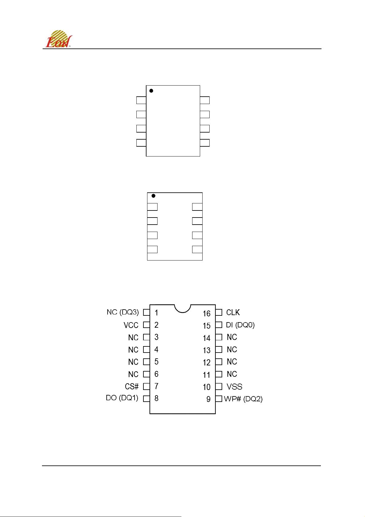
• Standard, Dual or Quad SPI
- Standard SPI: CLK, CS#, DI, DO, WP#
- Dual SPI: CLK, CS#, DQ
0
, DQ
1
, WP#
- Quad SPI: CLK, CS#, DQ
0
, DQ
1
, DQ
2
, DQ
3
• High performance
- 104MHz clock rate for one data bit
- 80MHz clock rate for two data bits
- 80MHz clock rate for four data bits
• Low power consumption
- 12 mA typical active current
- 1 μA typical power down current
• Uniform Sector Architecture:
- 1024 sectors of 4-Kbyte
- 64 blocks of 64-Kbyte
- Any sector or block can be erased individually
• Software and Hardware Write Protection:
- Write Protect all or portion of memory via
software
- Enable/Disable protection with WP# pin
• High performance program/erase speed
- Page program time: 0.8ms typical
- Sector erase time: 50ms typical
- Block erase time 200ms typical
- Chip erase time: 15 seconds typical
• Lockable 512 byte OTP security sector
• Minimum 100K endurance cycle
• Package Options
- 8 pins SOP 200mil body width
- 8 contact VDFN
- 16 pins SOP 300mil body width
- 24 balls BGA (6x8mm)
- All Pb-free packages are RoHS compliant
• Industrial temperature Range
GENERAL DESCRIPTION
The EN25Q32B is a 32 Megabit (4096K-byte) Serial Flash memory, with advanced write protection
mechanisms. The EN25Q32B supports the standard Serial Peripheral Interface (SPI), and a high
performance Dual output as well as Quad I/O using SPI pins: Serial Clock, Chip Select, Serial DQ
0
(DI),
DQ
1
(DO), DQ
2
(WP#) and DQ
3
(NC). SPI clock frequencies of up to 80MHz are supported allowing
equivalent clock rates of 160MHz for Dual Output and 320MHz for Quad Output when using the
Dual/Quad Output Fast Read instructions. The memory can be programmed 1 to 256 bytes at a time,
using the Page Program instruction.
The EN25Q32B is designed to allow either single
Sector/Block at a time or full chip erase operation. The
EN25Q32B can be configured to protect part of the memory as the software protected mode. The
device can sustain a minimum of 100K program/erase cycles on each sector
or block.
EN25Q32B
32 Me
g
abit Serial Flash Memor
y
with 4Kb
y
te Uniform Sector
This Data Sheet may be revised by subsequent versions ©2004 Eon Silicon Solution, Inc., www.eonssi.com
or modifications due to changes in technical specifications.
2
EN25Q32B
Rev. A
,
Issue Date: 2010
/
10
/
18
Figure.1 CONNECTION DIAGRAMS
8 - LEAD SOP
DO (DQ
1
)
WP# (DQ
2
)
VSS
CS#
DI (DQ
0
)
CLK
NC (DQ
3
)
VCC
1
2
3
4
8
7
6
5
8 - LEAD VDFN
DO (DQ
1
)
WP# (DQ
2
)
VSS
CS#
DI (DQ
0
)
CLK
NC (DQ
3
)
VCC
1
2
3
4
8
7
6
5
16 - LEAD SOP
This Data Sheet may be revised by subsequent versions ©2004 Eon Silicon Solution, Inc., www.eonssi.com
or modifications due to changes in technical specifications.
3
EN25Q32B
Rev. A
,
Issue Date: 2010
/
10
/
18
24 - Ball BGA
This Data Sheet may be revised by subsequent versions ©2004 Eon Silicon Solution, Inc., www.eonssi.com
or modifications due to changes in technical specifications.
4
EN25Q32B
Rev. A
,
Issue Date: 2010
/
10
/
18
Figure 2. BLOCK DIAGRAM
Note:
1. DQ
0
and DQ
1
are used for Dual and Quad instructions.
2. DQ
0
~ DQ
3
are used for Quad instructions.
This Data Sheet may be revised by subsequent versions ©2004 Eon Silicon Solution, Inc., www.eonssi.com
or modifications due to changes in technical specifications.
5
EN25Q32B
Rev. A
,
Issue Date: 2010
/
10
/
18
Table 1. Pin Names
Symbol Pin Name
CLK
Serial Clock Input
DI (DQ
0
)
Serial Data Input (Data Input Output 0)
*1
DO (DQ
1
)
Serial Data Output (Data Input Output 1)
*1
CS#
Chip Enable
WP# (DQ
2
)
Write Protect (Data Input Output 2)
*2
NC(DQ
3
)
Not Connect (Data Input Output 3)
*2
Vcc
Supply Voltage (2.7-3.6V)
Vss
Ground
NC
No Connect
Note:
1. DQ
0
and DQ
1
are used for Dual and Quad instructions.
2. DQ
0
~ DQ
3
are used for Quad instructions.
SIGNAL DESCRIPTION
Serial Data Input, Output and IOs (DI, DO and DQ
0
, DQ
1
, DQ
2
, DQ
3
)
The EN25Q32B support standard SPI, Dual SPI and Quad SPI operation. Standard SPI instructions
use the unidirectional DI (input) pin to serially write instructions, addresses or data to the device on the
rising edge of the Serial Clock (CLK) input pin. Standard SPI also uses the unidirectional DO (output) to
read data or status from the device on the falling edge CLK.
Dual and Quad SPI instruction use the bidirectional IO pins to serially write instruction, addresses or
data to the device on the rising edge of CLK and read data or status from the device on the falling edge
of CLK.
Serial Clock (CLK)
The SPI Serial Clock Input (CLK) pin provides the timing for serial input and output operations. ("See
SPI Mode")
Chip Select (CS#)
The SPI Chip Select (CS#) pin enables and disables device operation. When CS# is high the device is
deselected and the Serial Data Output (DO, or DQ
0
, DQ
1
, DQ
2
and DQ
3
) pins are at high impedance.
When deselected, the devices power consumption will be at standby levels unless an internal erase,
program or status register cycle is in progress. When CS# is brought low the device will be selected,
power consumption will increase to active levels and instructions can be written to and data read from
the device. After power-up, CS# must transition from high to low before a new instruction will be
accepted.
Write Protect (WP#)
The Write Protect (WP#) pin can be used to prevent the Status Register from being written. Used in
conjunction with the Status Register’s Block Protect (BP0, BP1, BP2 and BP3) bits and Status Register
Protect (SRP) bits, a portion or the entire memory array can be hardware protected. The WP# function
is only available for standard SPI and Dual SPI operation, when during Quad SPI, this pin is the Serial
Data IO (DQ
2
) for Quad I/O operation.
剩余54页未读,继续阅读
arktoo
- 粉丝: 0
- 资源: 2
上传资源 快速赚钱
- 我的内容管理 展开
- 我的资源 快来上传第一个资源
- 我的收益 登录查看自己的收益
- 我的积分 登录查看自己的积分
- 我的C币 登录后查看C币余额
- 我的收藏
- 我的下载
- 下载帮助
安全验证
文档复制为VIP权益,开通VIP直接复制
信息提交成功
- 1
- 2
前往页