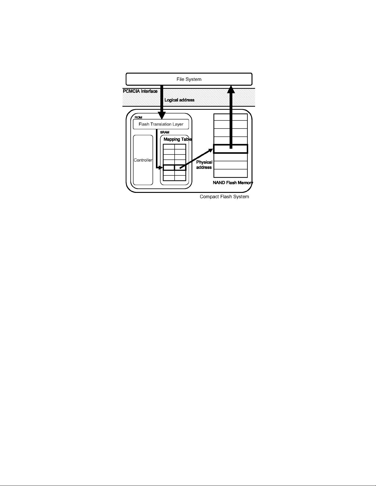
Log Buffer Based Flash Translation Layer


A Log Buffer-Based Flash Translation Layer
Using Fully-Associative Sector Translation
SANG-WON LEE
Sungkyunkwan University
DONG-JOO PARK
Soongsil University
TAE-SUN CHUNG
Ajou University
DONG-HO LEE
Hanyang University
SANGWON PARK
Hankook University of Foreign Studies
and
HA-JOO SONG
Pukyong National University
Flash memory is being rapidly deployed as data storage for mobile devices such as PDAs, MP3
players, mobile phones, and digital cameras, mainly because of its low electronic power, nonvolatile
storage, high performance, physical stability, and portability. One disadvantage of flash memory
is that prewritten data cannot be dynamically overwritten. Before overwriting prewritten data,
a time-consuming erase operation on the used blocks must precede, which significantly degrades
This work was supported in part by MIC & IITA through IT Leading R&D Support Project, in part
by MIC & IITA through Oversea Post-Doctoral Support Program 2005, in part by the Ministry
of Information and Communication, Korea under the ITRC support program supervised by the
Institute of Information Technology Assessment, IITA-2005-(C1090-0501-0019), and also supported
in part by Seoul R&D Program(10660).
Authors’ addresses: Sang-Won Lee, School of Information and Communications Engineering,
Sungkyunkwan University, Suwon 440-746, Korea; email: swlee@acm.org; Dong-Joo Park, School
of Computing, Soongsil University, Seoul 156-743, Korea; email: djpark@ssu.ac.kr; Tae-Sun
Chung, College of Information Technology, Ajou University, Suwon 443-749, Korea; email:
tschung@ajou.ac.kr; Dong-Ho Lee, Department of Computer Science and Engineering, Hanyang
University, Ansan 426-791, Korea; email: dhlee72@cse.hanyang.ac.kr; Sangwon Park, Informa-
tion Communication Engineering, Hankook University of Foreign Studies, Yongin 449-791, Korea;
email: swpark@hufs.ac.kr; Ha-Joo Song, Division of Electronic, Computer, and Telecommunication,
Pukyong National University, Busan 608-737, Korea; email: hajusong@pknu.ac.kr.
Permission to make digital or hard copies of part or all of this work for personal or classroom use is
granted without fee provided that copies are not made or distributed for profit or direct commercial
advantage and that copies show this notice on the first page or initial screen of a display along
with the full citation. Copyrights for components of this work owned by others than ACM must be
honored. Abstracting with credit is permitted. To copy otherwise, to republish, to post on servers,
to redistribute to lists, or to use any component of this work in other works requires prior specific
permission and/or a fee. Permissions may be requested from Publications Dept., ACM, Inc., 2 Penn
Plaza, Suite 701, New York, NY 10121-0701 USA, fax +1 (212) 869-0481, or permissions@acm.org.
C
2007 ACM 1539-9087/2007/07-ART18 $5.00 DOI 10.1145/1275986.1275990 http://doi.acm.org/
10.1145/1275986.1275990
ACM Transactions on Embedded Computing Systems, Vol. 6, No. 3, Article 18, Publication date: July 2007.


剩余26页未读,继续阅读
资源评论

 lowinrain2012-12-11很不错的论文,有深度
angelojiang
- 粉丝: 0
- 资源: 2


