没有合适的资源?快使用搜索试试~ 我知道了~
OP27(低噪声精密高速运算放大器).pdf
需积分: 50 16 下载量 135 浏览量
2021-01-05
10:46:30
上传
评论 1
收藏 324KB PDF 举报
温馨提示
试读
21页
失调电压低至25 µV,最大漂移为0.6 µV/°C,因而该器件是精密仪器仪表应用的理想之选。极低噪声(10 Hz时en=3.5nV/√Hz), 低1/f噪声转折频率(2.7Hz)以及高增益(180万),能够使低电平信号得到精确的高增益放大。
资源推荐
资源详情
资源评论
OP27A, OP27C, OP27E, OP27G
OP37A, OP37C, OP37E, OP37G
LOW-NOISE HIGH-SPEED PRECISION OPERATIONAL AMPLIFIERS
SLOS100B – FEBRUARY 1989 – REVISED AUGUST 1994
Copyright 1994, Texas Instruments Incorporated
2–1
POST OFFICE BOX 655303 • DALLAS, TEXAS 75265
POST OFFICE BOX 1443
• HOUSTON, TEXAS 77251–1443
• Direct Replacements for PMI and LTC OP27
and OP37 Series
Features of OP27A, OP27C, OP37A, and
OP37C:
• Maximum Equivalent Input Noise Voltage:
3.8 nV/√Hz
at 1 kHz
5.5 nV/√Hz
at 10 kHz
• Very Low Peak-to-Peak Noise Voltage at
0.1 Hz to 10 Hz . . . 80 nV Typ
• Low Input Offset Voltage ...25 µV Max
• High Voltage Amplification ...1 V/µV Min
Feature of OP37 Series:
• Minimum Slew Rate ...11 V/µs
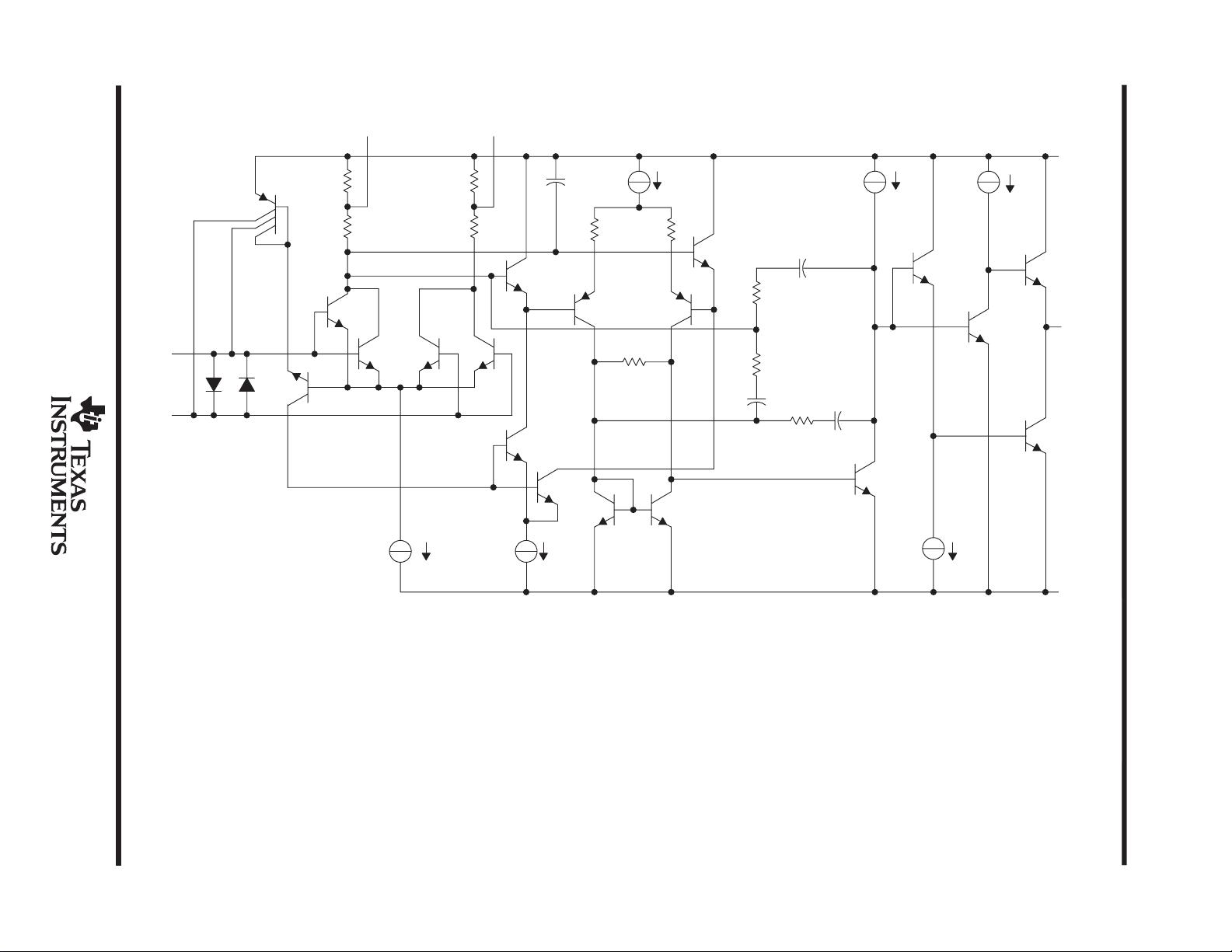
description
The OP27 and OP37 operational amplifiers
combine outstanding noise performance with
excellent precision and high-speed specifications.
The wideband noise is only 3 nV/√Hz
and with the
1/f noise corner at 2.7 Hz, low noise is maintained
for all low-frequency applications.
The outstanding characteristics of the OP27 and
OP37 make these devices excellent choices
for low-noise amplifier applications requiring
precision performance and reliability. Additionally,
the OP37 is free of latch-up in high-gain,
large-capacitive-feedback configurations.
The OP27 series is compensated for unity gain.
The OP37 series is decompensated for increased
bandwidth and slew rate and is stable down to a
gain of 5.
The OP27A, OP27C, OP37A, and OP37C are
characterized for operation over the full military
temperature range of –55°C to 125°C. The
OP27E, OP27G, OP37E, and OP37G are
characterized for operation from – 25°C to 85°C.
AVAILABLE OPTIONS
V
IO
max
STABLE
PACKAGE
T
A
V
IO
max
AT 25°C
STABLE
GAIN
CERAMIC DIP
(JG)
CHIP CARRIER
(FK)
PLASTIC DIP
(P)
25 µV
1 — — OP27EP
25
°
Cto85
°
C
25
µ
V
5 — — OP37EP
–
25°C
to
85°C
100 µV
1 — — OP27GP
100
µ
V
5 — — OP37GP
25 µV
1 OP27AJG OP27AFK —
55
°
Cto125
°
C
25
µ
V
5 OP37AJG OP37AFK —
–
55°C
to
125°C
100 µV
1 OP27CJG — —
100
µ
V
5 OP37CJG — —
PRODUCTION DATA information is current as of publication date.
Products conform to specifications per the terms of Texas Instruments
standard warranty. Production processing does not necessarily include
testing of all parameters.
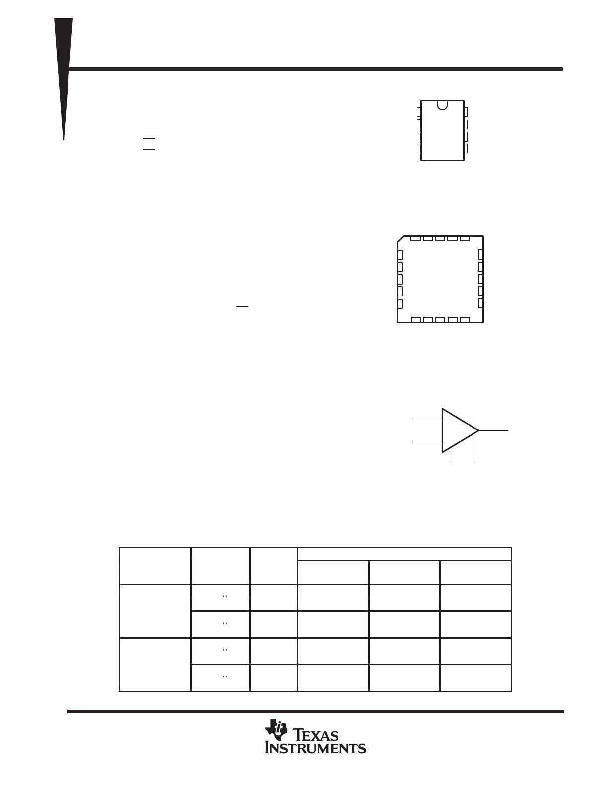
1
2
3
4
8
7
6
5
V
IO
TRIM
IN–
IN +
V
CC –
V
IO
TRIM
V
CC+
OUT
NC
JG OR P PACKAGE
(TOP VIEW)
IN+
IN –
OUT
V
IO
TRIM
18
6
3
2
symbol
3 2 1 20 19
910111213
4
5
6
7
8
18
17
16
15
14
NC
V
CC+
NC
OUT
NC
NC
1N–
NC
IN+
NC
FK PACKAGE
(TOP VIEW)
NC
NC
NC
NC
NC
NC
NC – No internal connection
CC –
V
Pin numbers are for the JG and P packages.
IO
V TRIM
NC
IO
V TRIM
+
–
OP27A, OP27C, OP27E, OP27G
OP37A, OP37C, OP37E, OP37G
LOW-NOISE HIGH-SPEED OPERATIONAL AMPLIFIER
SLOS100B – FEBRUARY 1989 – REVISED AUGUST 1994
2–2
POST OFFICE BOX 655303 DALLAS, TEXAS 75265POST OFFICE BOX 1443 HOUSTON, TEXAS 77251–1443
••
schematic
IN +
IN –
Q3
Q1A
Q1B Q2B Q2A
Q11
Q12
Q27 Q28
Q26
Q46
Q19
Q20
Q45
Q22
Q24Q23
Q21
Q6
V
IO
TRIM V
IO
TRIM
V
CC
+
OUT
V
CC
–
480 µA
750
µA
260
µA
240 µA 120
µA
340
µA
C1
†
†
C1 = 120 pF for OP27
C1 = 15 pF for OP37
OP27A, OP27C, OP27E, OP27G
OP37A, OP37C, OP37E, OP37G
LOW-NOISE HIGH-SPEED PRECISION OPERATIONAL AMPLIFIERS
SLOS100B – FEBRUARY 1989 – REVISED AUGUST 1994
2–3
POST OFFICE BOX 655303 • DALLAS, TEXAS 75265
POST OFFICE BOX 1443
• HOUSTON, TEXAS 77251–1443
absolute maximum ratings over operating free-air temperature range (unless otherwise noted)
Supply voltage, V
CC+
(see Note 1) 22 V. . . . . . . . . . . . . . . . . . . . . . . . . . . . . . . . . . . . . . . . . . . . . . . . . . . . . . . . . .
Supply voltage, V
CC–
(see Note 1) – 22 V. . . . . . . . . . . . . . . . . . . . . . . . . . . . . . . . . . . . . . . . . . . . . . . . . . . . . . . . .
Input voltage, V
I
V
CC±
. . . . . . . . . . . . . . . . . . . . . . . . . . . . . . . . . . . . . . . . . . . . . . . . . . . . . . . . . . . . . . . . . . . . . . . . .
Duration of output short circuit unlimited. . . . . . . . . . . . . . . . . . . . . . . . . . . . . . . . . . . . . . . . . . . . . . . . . . . . . . . . . . .
Differential input current (see Note 2) ±25 mA. . . . . . . . . . . . . . . . . . . . . . . . . . . . . . . . . . . . . . . . . . . . . . . . . . . . .
Continuous power dissipation See Dissipation Rating Table. . . . . . . . . . . . . . . . . . . . . . . . . . . . . . . . . . . . . . . . .
Operating free-air temperature range: OP27A, OP27C, OP37A, OP37C – 55°C to 125°C. . . . . . . . . . . . . . .
OP27E, OP27G, OP37E, OP37G – 25°C to 85°C. . . . . . . . . . . . . . .
Storage temperature range – 65°C to 150°C. . . . . . . . . . . . . . . . . . . . . . . . . . . . . . . . . . . . . . . . . . . . . . . . . . . . . . .
Lead temperature 1,6 mm (1/16 inch) from case for 60 seconds: JG or FK package 300°C. . . . . . . . . . . . . .
Lead temperature 1,6 mm (1/16 inch) from case for 10 seconds : P package 260°C. . . . . . . . . . . . . . . . . . . .
NOTES: 1. All voltage values are with respect to the midpoint between V
CC+
and V
CC–
unless otherwise noted.
2. The inputs are protected by back-to-back diodes. Current-limiting resistors are not used in order to achieve low noise. Excessive
input current will flow if a differential input voltage in excess of approximately ± 0.7 V is applied between the inputs unless some
limiting resistance is used.
DISSIPATION RATING TABLE
PACKAGE
T
A
≤ 25°C
POWER RATING
DERATING FACTOR
ABOVE T
A
= 25°C
T
A
= 85°C
POWER RATING
T
A
= 125°C
POWER RATING
JG
FK
P
1050 mW
1375 mW
1000 mW
8.4 mW/°C
11.0 mW/°C
8.0 mW/°C
546 mW
715 mW
520 mW
210 mW
275 mW
N/A
OP27A, OP27C, OP27E, OP27G
OP37A, OP37C, OP37E, OP37G
LOW-NOISE HIGH-SPEED PRECISION OPERATIONAL AMPLIFIERS
SLOS100B – FEBRUARY 1989 – REVISED AUGUST 1994
2–4
POST OFFICE BOX 655303 • DALLAS, TEXAS 75265
POST OFFICE BOX 1443
• HOUSTON, TEXAS 77251–1443
recommended operating conditions
OP27A, OP37A OP27C, OP37C
UNIT
MIN NOM MAX MIN NOM MAX
UNIT
Supply voltage, V
CC+
4 15 22 4 15 22 V
Supply voltage, V
CC–
–4 –15 –22 –4 –15 –22 V
Common mode in
p
ut voltage V
IC
V
CC±
= ± 15 V, T
A
= 25°C ± 11 ± 11
V
Common
-
mode
inp
u
t
v
oltage
,
V
IC
V
CC±
= ± 15 V, T
A
= – 55°C to 125°C ±10.3 ±10.2
V
Operating free-air temperature, T
A
–55 125 –55 125 °C
electrical characteristics at specified free-air temperature, V
CC±
= ±15 V (unless otherwise noted)
PARAMETER
TEST CONDITIONS
T
†
OP27A, OP37A OP27C, OP37C
UNIT
PARAMETER
TEST
CONDITIONS
T
A
†
MIN TYP MAX MIN TYP MAX
UNIT
V
IO
In
p
ut offset voltage
V
O
= 0, V
IC
= 0
25°C 10 25 30 100
µV
V
IO
Inp
u
t
offset
v
oltage
O
,
IC
R
S
= 50 Ω, See Note 3
Full range 60 300
µ
V
α
VIO
Average temperature
coefficient of input
offset voltage
Full range 0.2 0.6 0.4 1.8 µV/°C
Long-term drift of input
offset voltage
See Note 4 0.2 1 0.4 2 µV/mo
I
IO
In
p
ut offset current
V
O
=0 V
IC
=0
25°C 7 35 12 75
nA
I
IO
Inp
u
t
offset
c
u
rrent
V
O
=
0
,
V
IC
=
0
Full range 50 135
nA
I
IB
In
p
ut bias current
V
O
=0 V
IC
=0
25°C ±10 ±40 ±15 ±80
nA
I
IB
Inp
u
t
bias
c
u
rrent
V
O
=
0
,
V
IC
=
0
Full range ±60 ±150
nA
V
ICR
Common-mode input
25°C
11
to
–11
11
to
–11
V
V
ICR
voltage range
Full range
10.3
to
–10.3
10.5
to
–10.5
V
R
L
≥ 2 kΩ ±12 ±13.8 ±11.5 ±13.5
V
OM
Peak output voltage swing
R
L
≥ 0.6 kΩ
±10 ±11.5 ±10 ±11.5
V
R
L
≥ 2 kΩ Full range ±11.5 10.5
R
L
≥ 2 kΩ, V
O
= ±10 V 1000 1800 700 1500
Large signal differential
R
L
≥ 1 kΩ, V
O
= ±10 V 800 1500 1500
A
VD
Large
-
signal
differential
voltage amplification
R
L
≥ 0.6 kΩ, V
O
= ±1 V,
V
CC±
= ± 4 V
250 700 200 500
V/mV
R
L
≥ 2 kΩ, V
O
= ±10 V Full range 600 300
r
i(CM)
Common-mode input
resistance
3 2 GΩ
r
o
Output resistance V
O
= 0, I
O
= 0 25°C 70 70 Ω
CMRR
Common-mode rejection
V
IC
= ±11 V 25°C 114 126 100 120
dB
CMRR
j
ratio
V
IC
= ±10 V
Full range 110 94
dB
k
SVR
Supply voltage rejection
V
CC±
= ±4 V to ±18 V 25°C 100 120 94 118
dB
k
SVR
ygj
ratio
V
CC±
= ±4.5 V to ±18 V Full range 96 86
dB
†
Full range is – 55°C to 125°C.
NOTES: 3. Input offset voltage measurements are performed by automatic test equipment approximately 0.5 seconds after applying power.
4. Long-term drift of input offset voltage refers to the average trend line of offset voltage versus time over extended periods after the
first 30 days of operation. Excluding the initial hour of operation, changes in V
IO
during the first 30 days are typically 2.5 µV
(see Figure 3).
OP27A, OP27C, OP27E, OP27G
OP37A, OP37C, OP37E, OP37G
LOW-NOISE HIGH-SPEED PRECISION OPERATIONAL AMPLIFIERS
SLOS100B – FEBRUARY 1989 – REVISED AUGUST 1994
2–5
POST OFFICE BOX 655303 • DALLAS, TEXAS 75265
POST OFFICE BOX 1443
• HOUSTON, TEXAS 77251–1443
recommended operating conditions
MIN NOM MAX UNIT
Supply voltage, V
CC+
4 15 22 V
Supply voltage, V
CC –
–4 –15 –22 V
Common mode in
p
ut voltage V
IC
V
CC±
= ±15 V, T
A
= 25°C ±11
V
Common
-
mode
inp
u
t
v
oltage
,
V
IC
V
CC±
= ±15 V, T
A
= – 55°C to 125°C ±10.5
V
Operating free-air temperature, T
A
–25 85 °C
electrical characteristics at specified free-air temperature, V
CC
±
= ±15 V (unless otherwise noted)
PARAMETER
TEST CONDITIONS
T
†
OP27E, OP37E OP27G, OP37G
UNIT
PARAMETER
TEST
CONDITIONS
T
A
†
MIN TYP MAX MIN TYP MAX
UNIT
V
IO
In
p
ut offset voltage
V
O
= 0, V
IC
= 0
25°C 10 25 30 100
µV
V
IO
Inp
u
t
offset
v
oltage
O
,
IC
R
S
= 50 Ω, See Note 3
Full range 60 220
µ
V
αV
IO
Average temperature
coefficient of input
offset voltage
Full range 0.2 0.6 0.4 1.8 µV/°C
Long-term drift of input
offset voltage
See Note 4 0.2 1 0.4 2 µV/mo
I
IO
In
p
ut offset current
V
O
=0 V
IC
=0
25°C 7 35 12 75
nA
I
IO
Inp
u
t
offset
c
u
rrent
V
O
=
0
,
V
IC
=
0
Full range 50 135
nA
I
IB
In
p
ut bias current
V
O
=0 V
IC
=0
25°C ±10 ±40 ±15 ±80
nA
I
IB
Inp
u
t
bias
c
u
rrent
V
O
=
0
,
V
IC
=
0
Full range ±60 ±150
nA
V
ICR
Common-mode input
25°C
11
to
–11
11
to
–11
V
V
ICR
voltage range
Full range
10.3
to
–10.3
10.5
to
–10.5
V
R
L
≥ 2 kΩ ±12 ±13.8 ±11.5 ±13.5
V
OM
Peak output voltage swing
R
L
≥ 0.6 kΩ
±10 ±11.5 ±10 ±11.5
V
R
L
≥ 2 kΩ Full range ±11.5 10.5
R
L
≥ 2 kΩ, V
O
= ±10 V 1000 1800 700 1500
Large signal differential
R
L
≥ 1 kΩ, V
O
= ±10 V 800 1500 1500
A
VD
Large
-
signal
differential
voltage amplification
R
L
≥ 0.6 kΩ, V
O
= ±1 V,
V
CC±
= ± 4 V
250 700 200 500
V/mV
R
L
≥ 2 kΩ, V
O
= ± 10 V Full range 600 450
r
i(CM)
Common-mode input
resistance
3 2 GΩ
r
o
Output resistance V
O
= 0, I
O
= 0 25°C 70 70 Ω
CMRR
Common-mode rejection
V
IC
= ±11 V 25°C 114 126 100 120
dB
CMRR
j
ratio
V
IC
= ±10 V
Full range 110 96
dB
k
SVR
Supply voltage rejection
V
CC±
= ± 4 V to ±18 V 25°C 100 120 94 118
dB
k
SVR
ygj
ratio
V
CC±
= ± 4.5 V to ±18 V Full range 96 90
dB
†
Full range is – 25°C to 85°C.
NOTES: 3. Input offset voltage measurements are performed by automatic test equipment approximately 0.5 seconds after applying power.
4. Long-term drift of input offset voltage refers to the average trend line of offset voltage versus time over extended periods after the
first 30 days of operation. Excluding the initial hour of operation, changes in V
IO
during the first 30 days are typically 2.5 µV
(see Figure 3).
剩余20页未读,继续阅读
资源评论
ZLI960117
- 粉丝: 9
- 资源: 74
上传资源 快速赚钱
- 我的内容管理 展开
- 我的资源 快来上传第一个资源
- 我的收益 登录查看自己的收益
- 我的积分 登录查看自己的积分
- 我的C币 登录后查看C币余额
- 我的收藏
- 我的下载
- 下载帮助
安全验证
文档复制为VIP权益,开通VIP直接复制
信息提交成功