CC2530 datasheet
需积分: 10 153 浏览量
2009-09-21
16:11:03
上传
评论
收藏 884KB PDF 举报


1
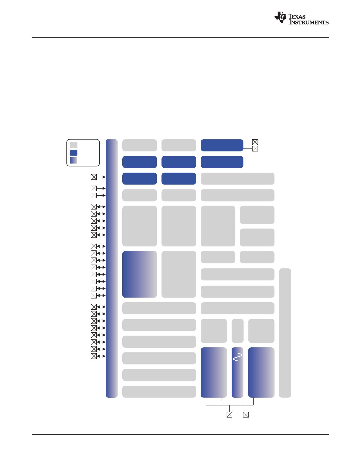
FEATURES
APPLICATIONS
CC2530F32 , CC2530F64 , CC2530F128 , CC2530F256
www.ti.com
.......................................................................................................................................................... SWRS081A – APRIL 2009 – REVISED APRIL 2009
A True System-on-Chip Solution for 2.4-GHz IEEE 802.15.4 and ZigBee Applications
– Accurate Digital RSSI/LQI Support
2345
• RF/Layout – Battery Monitor and Temperature Sensor
– 2.4-GHz IEEE 802.15.4 Compliant RF – 12-Bit ADC With Eight Channels and
Transceiver Configurable Resolution
– Excellent Receiver Sensitivity and – AES Security Coprocessor
Robustness to Interference
– Two Powerful USARTs With Support for
– Programmable Output Power Up to 4.5 dBm Several Serial Protocols
– Very Few External Components – 21 General-Purpose I/O Pins (19 × 4 mA, 2 ×
20 mA)
– Only a Single Crystal Needed for Mesh
Network Systems – Watchdog Timer
– 6-mm × 6-mm QFN40 Package • Development Tools
– Suitable for Systems Targeting Compliance – CC2530 Development Kit
With Worldwide Radio-Frequency
– CC2530 ZigBee
®
Development Kit
Regulations: ETSI EN 300 328 and EN 300
– CC2530 RemoTI™ Development Kit for
440 (Europe), FCC CFR47 Part 15 (US) and
RF4CE
ARIB STD-T-66 (Japan)
– SmartRF™ Software
• Low Power
– Packet Sniffer
– Active-Mode RX (CPU Idle): 24 mA
– IAR Embedded Workbench™ Available
– Active Mode TX at 1 dBm (CPU Idle): 29 mA
– Power Mode 1 (4 µ s Wake-Up): 0.2 mA
– Power Mode 2 (Sleep Timer Running): 1 µ A
• 2.4-GHz IEEE 802.15.4 Systems
– Power Mode 3 (External Interrupts): 0.4 µ A
• RF4CE Remote Control Systems (64-KB Flash
and Higher)
– Wide Supply-Voltage Range (2 V – 3.6 V)
• ZigBee Systems (256-KB Flash)
• Microcontroller
• Home/Building Automation
– High-Performance and Low-Power 8051
• Lighting Systems
Microcontroller Core With Code Prefetch
• Industrial Control and Monitoring
– 32-, 64-, 128-, or 256-KB
• Low-Power Wireless Sensor Networks
In-System-Programmable Flash
• Consumer Electronics
– 8-KB RAM With Retention in All Power
• Health Care
Modes
– Hardware Debug Support
• Peripherals
– Powerful Five-Channel DMA
– IEEE 802.15.4 MAC Timer, General-Purpose
Timers (One 16-Bit, Two 8-Bit)
– IR Generation Circuitry
– 32-kHz Sleep Timer With Capture
– CSMA/CA Hardware Support
1
Please be aware that an important notice concerning availability, standard warranty, and use in critical applications of Texas
Instruments semiconductor products and disclaimers thereto appears at the end of this data sheet.
2 RemoTI, SmartRF, Z-Stack are trademarks of Texas Instruments.
3 IAR Embedded Workbench is a trademark of IAR Systems AB.
4 ZigBee is a registered trademark of the ZigBee Alliance.
5 All other trademarks are the property of their respective owners.
PRODUCTION DATA information is current as of publication date.
Copyright © 2009, Texas Instruments Incorporated
Products conform to specifications per the terms of the Texas
Instruments standard warranty. Production processing does not
necessarily include testing of all parameters.


剩余30页未读,继续阅读


评论0
最新资源