[AK09918]
016014242-E-00 2016/11
- 2 -
3. Table of Contents
1. General Description .................................................................................................................. 1
2. Features ..................................................................................................................................... 1
3. Table of Contents ...................................................................................................................... 2
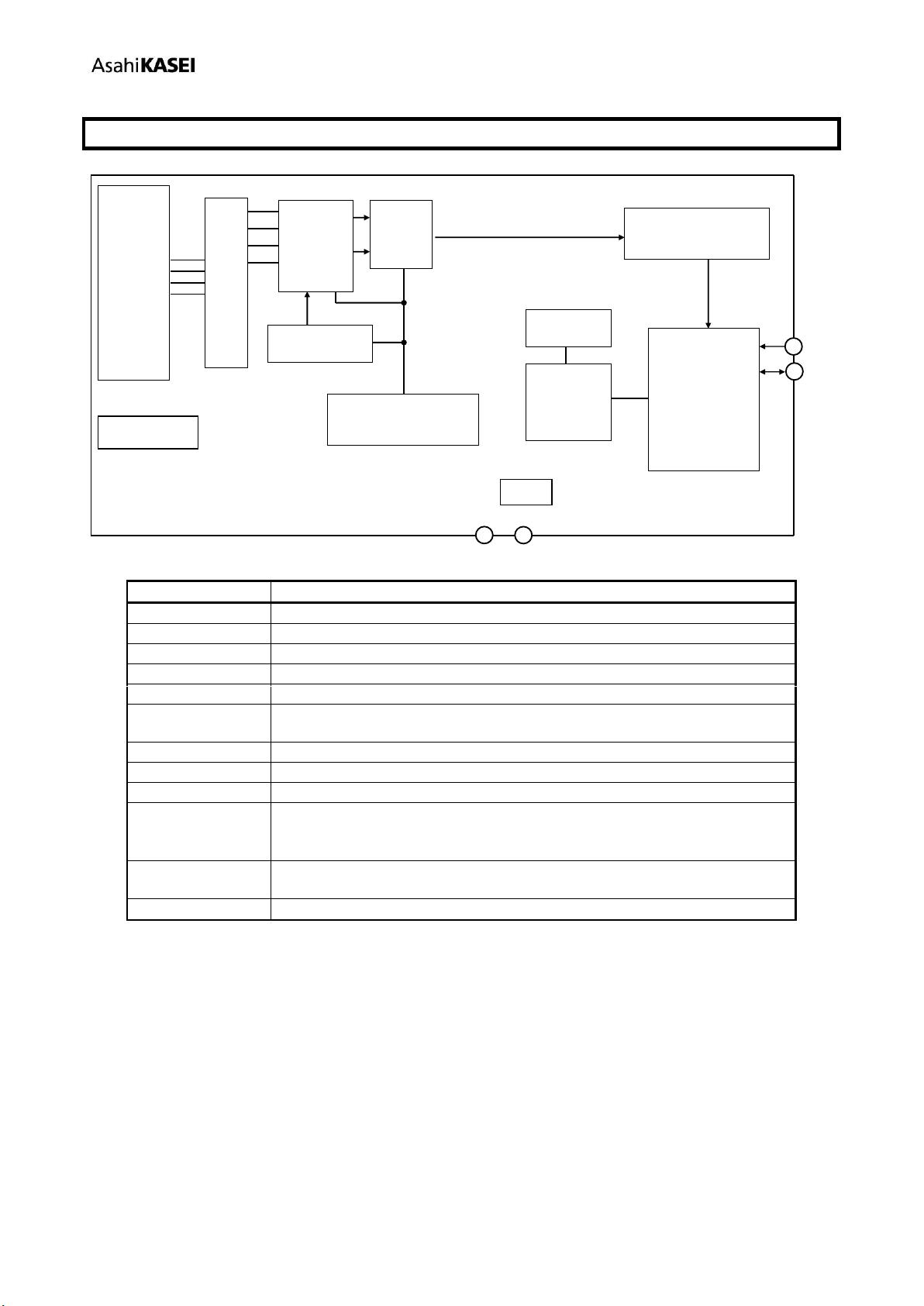
4. Block Diagram and Functions ................................................................................................... 3
5. Pin Configurations and Functions ............................................................................................. 4
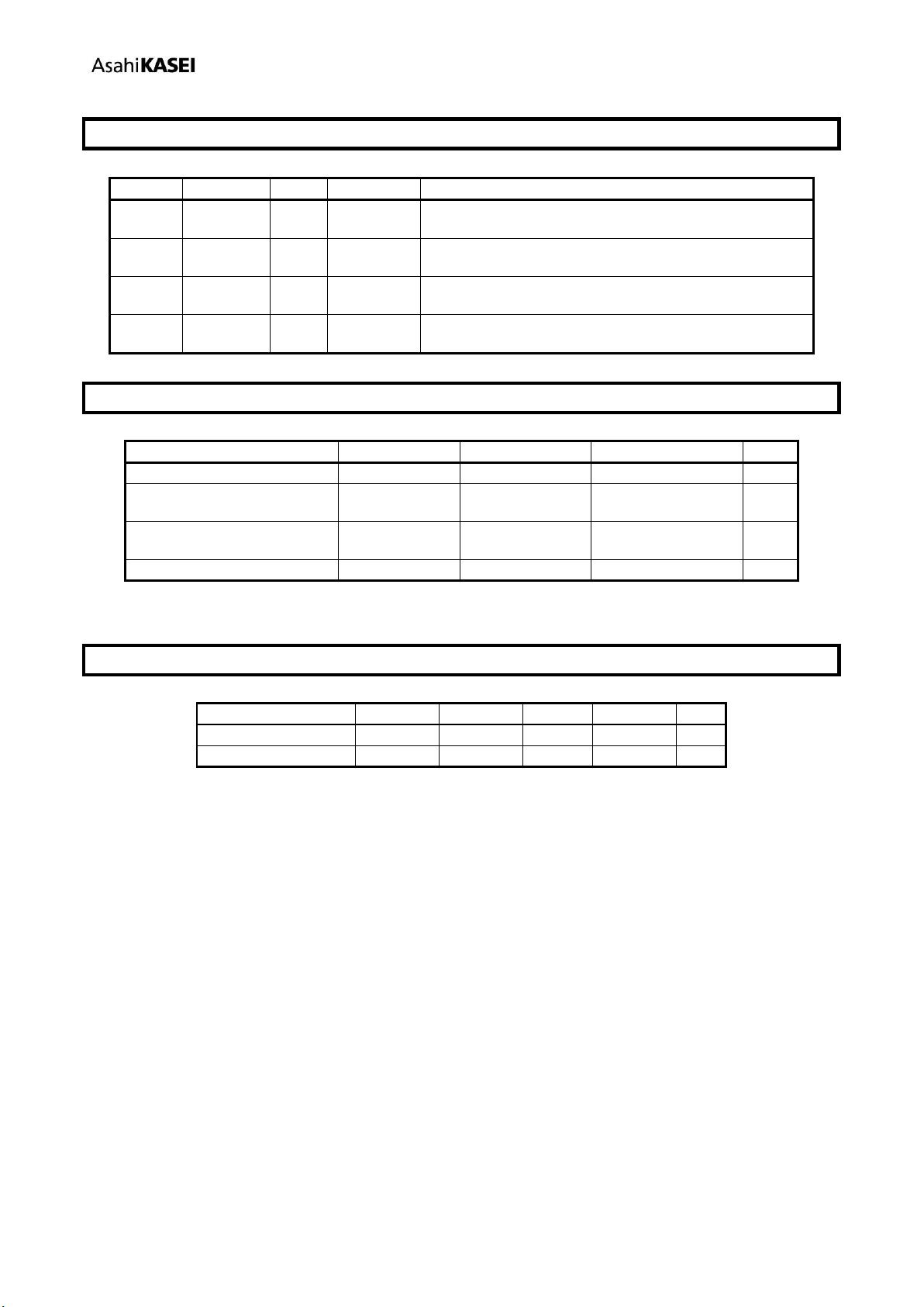
6. Absolute Maximum Ratings ...................................................................................................... 4
7. Recommended Operating Conditions ....................................................................................... 4
8. Electrical Characteristics ........................................................................................................... 5
8.1. DC Characteristics .............................................................................................................. 5
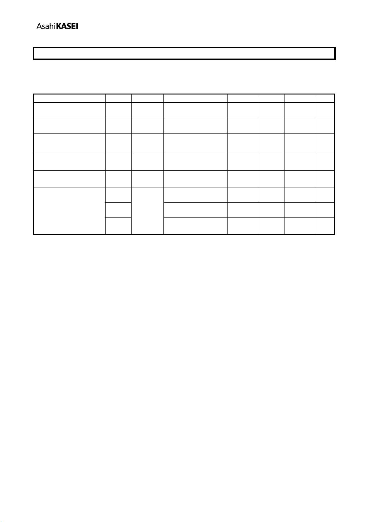
8.2. AC Characteristics .............................................................................................................. 6
8.3. Analog Circuit Characteristics ............................................................................................ 6
8.4. I
2
C Bus Interface ................................................................................................................ 7
9. Function Descriptions ............................................................................................................... 8
9.1. Power States ....................................................................................................................... 8
9.2. Reset Functions .................................................................................................................. 8
9.3. Operation Modes ................................................................................................................ 9
9.4. Description of Each Operation Mode ............................................................................... 10
Power-down Mode .................................................................................................... 10 9.4.1.
Single Measurement Mode ........................................................................................ 10 9.4.2.
Continuous Measurement Mode 1, 2, 3 and 4 ........................................................... 11 9.4.3.
Self-test Mode............................................................................................................ 15 9.4.4.
10. Serial Interface ...................................................................................................................... 16
10.1. I
2
C Bus Interface ............................................................................................................ 16
Data Transfer ........................................................................................................... 16 10.1.1.
WRITE Instruction .................................................................................................. 18
10.1.2.
READ Instruction .................................................................................................... 19 10.1.3.
11. Registers ................................................................................................................................ 20
11.1. Description of Registers ................................................................................................. 20
11.2. Register Map .................................................................................................................. 21
11.3. Detailed Description of Register .................................................................................... 22
WIA: Who I Am ...................................................................................................... 22 11.3.1.
RSV: Reserved register ............................................................................................ 22 11.3.2.
ST1: Status 1 ............................................................................................................ 22 11.3.3.
HXL to HZH: Measurement data ............................................................................ 23 11.3.4.
TMPS: Dummy register ........................................................................................... 23 11.3.5.
ST2: Status 2 ............................................................................................................ 24 11.3.6.
CNTL1: Dummy register ......................................................................................... 24 11.3.7.
CNTL2: Control 2 .................................................................................................... 24
11.3.8.
CNTL3: Control 3 .................................................................................................... 25 11.3.9.
TS1, TS2: Test register........................................................................................... 25 11.3.10.
12. Example of Recommended External Connection ................................................................. 26
13. Package ................................................................................................................................. 27
13.1. Marking .......................................................................................................................... 27
13.2. Pin Assignment ............................................................................................................... 27
13.3. Outline Dimensions ........................................................................................................ 28
13.4. Recommended Foot Print Pattern ................................................................................... 28
14. Relationship between the Magnetic Field and Output Code ................................................. 29
IMPORTANT NOTICE .............................................................................................................. 30