24C02CEEPROM使用手册
需积分: 9 71 浏览量
2009-10-16
20:35:22
上传
评论
收藏 102KB PDF 举报


1997 Microchip Technology Inc.
Preliminary
DS21202A-page 1
M
24C02C
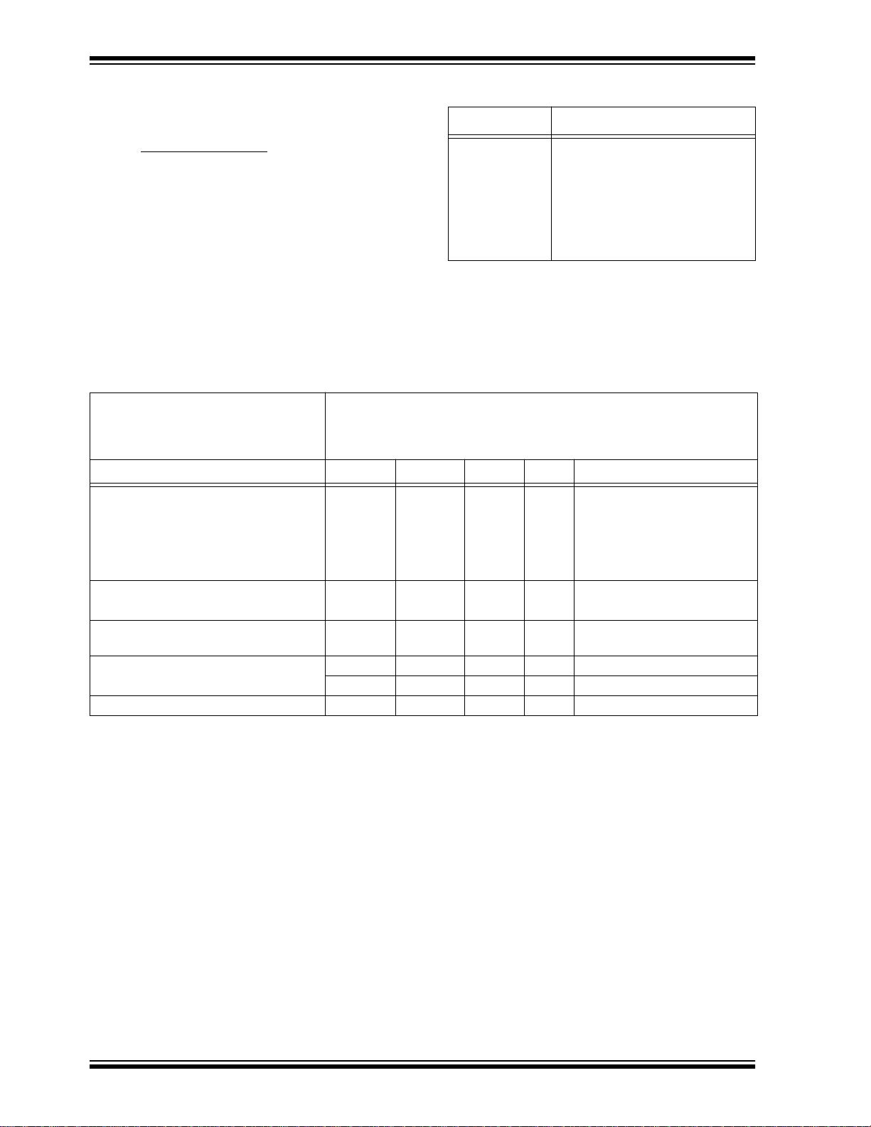
FEATURES
• Single supply with operation from 4.5 to 5.5V
• Low power CMOS technology
- 1 mA active current typical
- 10
µ
A standby current typical at 5.5V
• Organized as a single block of 256 bytes (256 x 8)
• Hardware write protection for upper half of array
• 2-wire serial interface bus, I
2
C compatible
• 100 kHz and 400 kHz compatibility
• Page-write buffer for up to 16 bytes
• Self-timed write cycle (including auto-erase)
• Fast 1 mS write cycle time for byte or page mode
• Address lines allow up to eight devices on bus
• 1,000,000 erase/write cycles guaranteed
• ESD protection > 4,000V
• Data retention > 200 years
• 8-pin PDIP, SOIC or TSSOP packages
• Available for extended temperature ranges
DESCRIPTION
The Microchip Technology Inc. 24C02C is a 2K bit
Serial Electrically Erasable PROM with a voltage range
of 4.5V to 5.5V. The device is organized as a single
block of 256 x 8-bit memory with a 2-wire serial inter-
face. Low current design permits operation with typical
standby and active currents of only 10
µ
A and 1 mA
respectively. The device has a page-write capability for
up to 16 bytes of data and has fast write cycle times of
only 1 mS for both byte and page writes. Functional
address lines allow the connection of up to eight
24C02C devices on the same bus for up to 16K bits of
contiguous EEPROM memory. The device is available
in the standard 8-pin PDIP, 8-pin SOIC (150 mil), and
TSSOP packages.
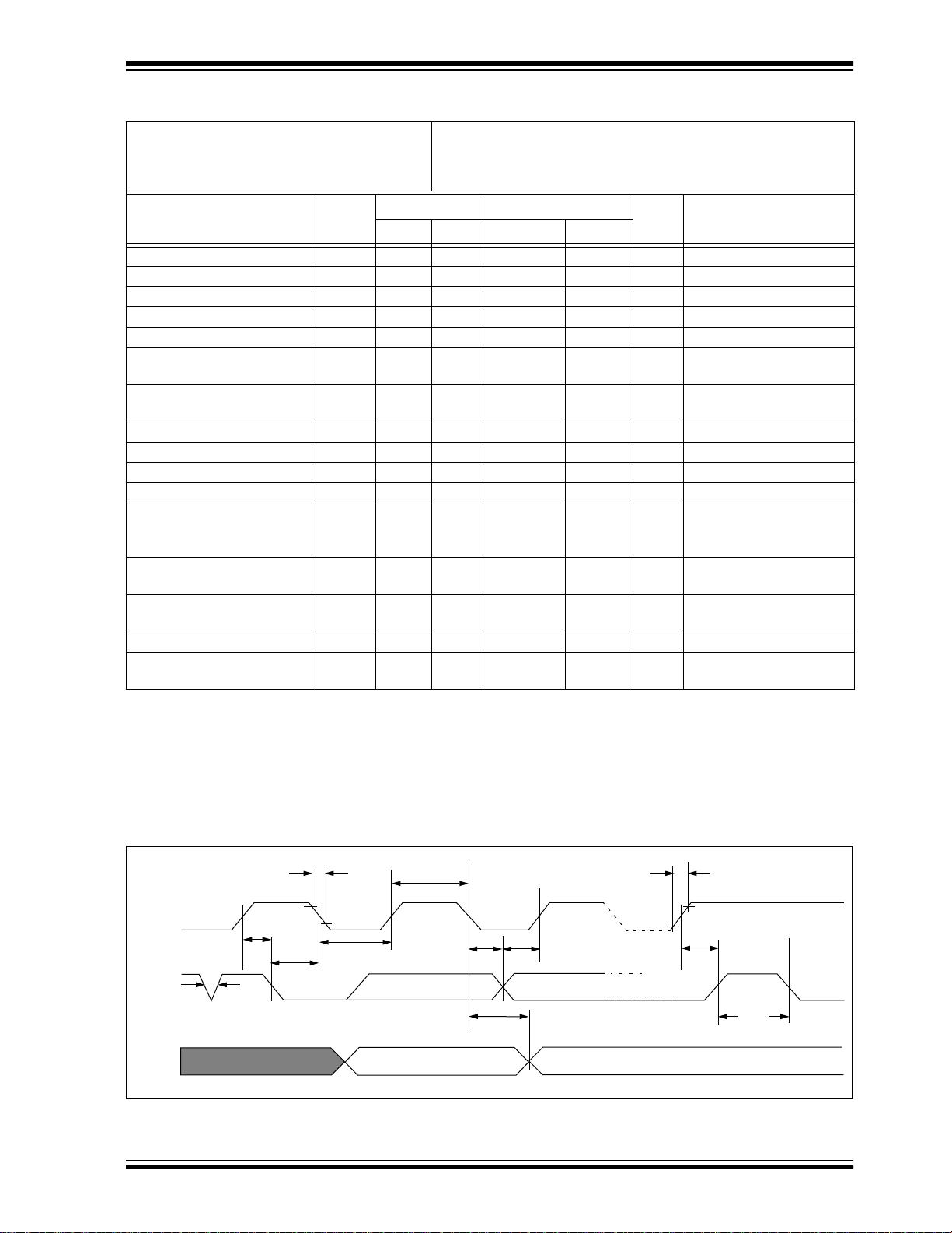
PACKAGE TYPES
BLOCK DIAGRAM
- Commercial (C): 0
°
C to +70
°
C
- Industrial (I): -40
°
C to +85
°
C
- Automotive (E): -40
°
C to +125
°
C
PDIP/SOIC
TSSOP
A0
A1
A2
Vss
Vcc
WP
SCL
SDA
24C02C
24C02C
1
2
3
4
8
7
6
5
A0
A1
A2
V
SS
VCC
WP
SCL
SDA
1
2
3
4
8
7
6
5
I/O
Control
Logic
Memory
Control
Logic
XDEC
HV Generator
EEPROM
Array
Write Protect
Circuitry
YDEC
Vcc
Vss
SENSE AMP
R/W CONTROL
SDA
SCL
A0 A1 A2
WP
2K 5.0V I
2
C
™
Serial EEPROM
I
2
C is a trademark of Philips Corporation.
查询24C02C供应商
剩余11页未读,继续阅读


评论0