


DATA SHEET
Product specification
Supersedes data of 1997 Apr 02
File under Integrated Circuits, IC12
1998 Jul 02
INTEGRATED CIRCUITS
PCF8591
8-bit A/D and D/A converter

1998 Jul 02 2
Philips Semiconductors Product specification
8-bit A/D and D/A converter PCF8591
CONTENTS
1 FEATURES
2 APPLICATIONS
3 GENERAL DESCRIPTION
4 ORDERING INFORMATION
5 BLOCK DIAGRAM
6 PINNING
7 FUNCTIONAL DESCRIPTION
7.1 Addressing
7.2 Control byte
7.3 D/A conversion
7.4 A/D conversion
7.5 Reference voltage
7.6 Oscillator
8 CHARACTERISTICS OF THE I
2
C-BUS
8.1 Bit transfer
8.2 Start and stop conditions
8.3 System configuration
8.4 Acknowledge
8.5 I
2
C-bus protocol
9 LIMITING VALUES
10 HANDLING
11 DC CHARACTERISTICS
12 D/A CHARACTERISTICS
13 A/D CHARACTERISTICS
14 AC CHARACTERISTICS
15 APPLICATION INFORMATION
16 PACKAGE OUTLINES
17 SOLDERING
17.1 Introduction
17.2 DIP
17.2.1 Soldering by dipping or by wave
17.2.2 Repairing soldered joints
17.3 SO
17.3.1 Reflow soldering
17.3.2 Wave soldering
17.3.3 Repairing soldered joints
18 DEFINITIONS
19 LIFE SUPPORT APPLICATIONS
20 PURCHASE OF PHILIPS I
2
C COMPONENTS
1998 Jul 02 3
Philips Semiconductors Product specification
8-bit A/D and D/A converter PCF8591
1 FEATURES
• Single power supply
• Operating supply voltage 2.5 V to 6 V
• Low standby current
• Serial input/output via I
2
C-bus
• Address by 3 hardware address pins
• Sampling rate given by I
2
C-bus speed
• 4 analog inputs programmable as single-ended or
differential inputs
• Auto-incremented channel selection
• Analog voltage range from V
SS
to V
DD
• On-chip track and hold circuit
• 8-bit successive approximation A/D conversion
• Multiplying DAC with one analog output.
2 APPLICATIONS
• Closed loop control systems
• Low power converter for remote data acquisition
• Battery operated equipment
• Acquisition of analog values in automotive, audio and
TV applications.
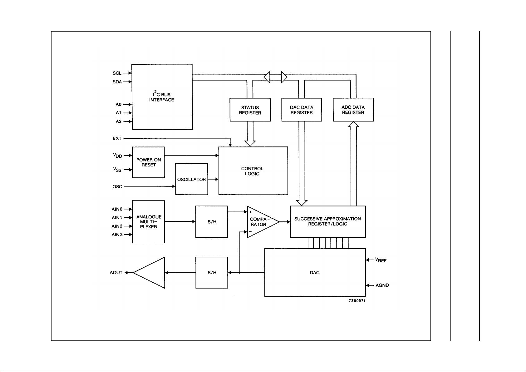
3 GENERAL DESCRIPTION
The PCF8591 is a single-chip, single-supply low power
8-bit CMOS data acquisition device with four analog
inputs, one analog output and a serial I
2
C-bus interface.
Three address pins A0, A1 and A2 are used for
programming the hardware address, allowing the use of
up to eight devices connected to the I
2
C-bus without
additional hardware. Address, control and data to and from
the device are transferred serially via the two-line
bidirectional I
2
C-bus.
The functions of the device include analog input
multiplexing, on-chip track and hold function, 8-bit
analog-to-digital conversion and an 8-bit digital-to-analog
conversion. The maximum conversion rate is given by the
maximum speed of the I
2
C-bus.
4 ORDERING INFORMATION
TYPE
NUMBER
PACKAGE
NAME DESCRIPTION VERSION
PCA8591P DIP16 plastic dual in-line package; 16 leads (300 mil); long body SOT38-1
PCA8591T SO16 plastic small outline package; 16 leads; body width 7.5 mm SOT162-1
1998 Jul 02 4
Philips Semiconductors Product specification
8-bit A/D and D/A converter PCF8591
This text is here in white to force landscape pages to be rotated correctly when browsing through the pdf in the Acrobat reader.This text is here in
_white to force landscape pages to be rotated correctly when browsing through the pdf in the Acrobat reader.This text is here inThis text is here in
white to force landscape pages to be rotated correctly when browsing through the pdf in the Acrobat reader. white to force landscape pages to be ...
5 BLOCK DIAGRAM
Fig.1 Block diagram.
1998 Jul 02 5
Philips Semiconductors Product specification
8-bit A/D and D/A converter PCF8591
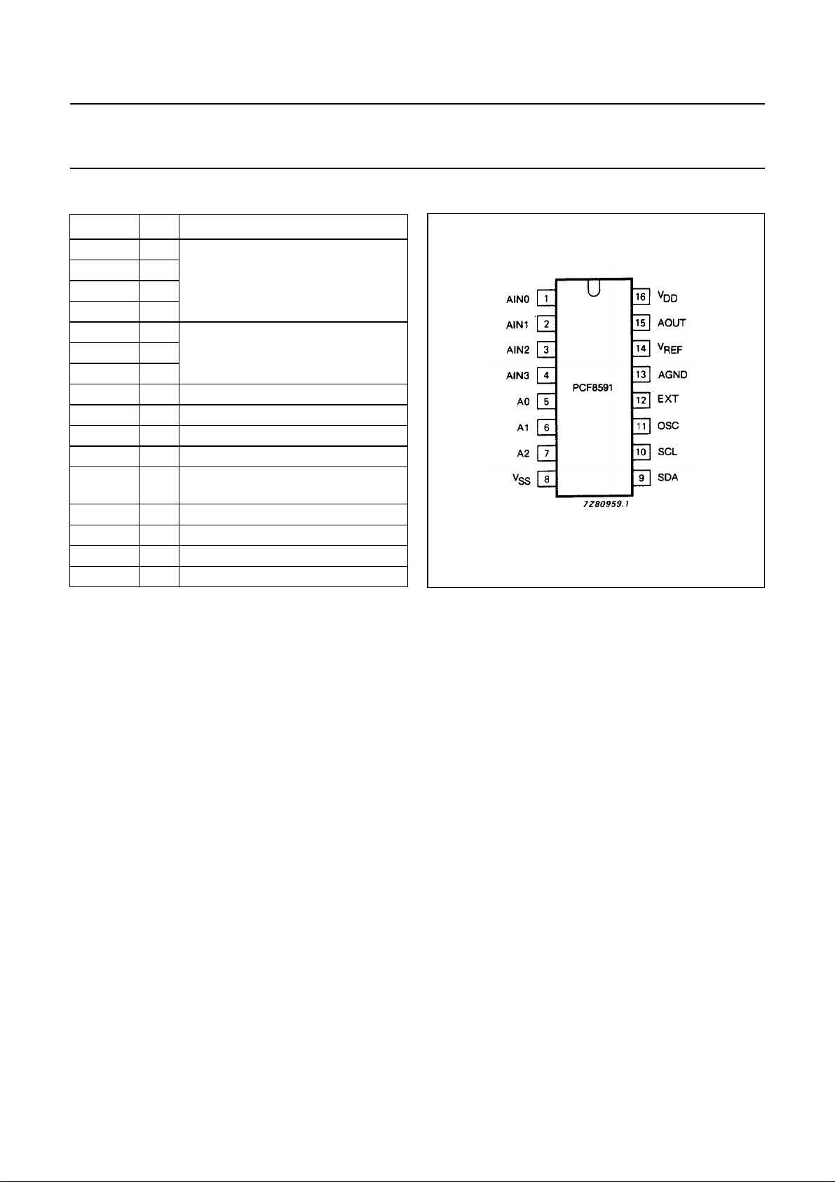
6 PINNING
SYMBOL PIN DESCRIPTION
AINO 1
analog inputs
(A/D converter)
AIN1 2
AIN2 3
AIN3 4
A0 5
hardware addressA1 6
A2 7
V
SS
8 negative supply voltage
SDA 9 I
2
C-bus data input/output
SCL 10 I
2
C-bus clock input
OSC 11 oscillator input/output
EXT 12 external/internal switch for oscillator
input
AGND 13 analog ground
V
REF
14 voltage reference input
AOUT 15 analog output (D/A converter)
V
DD
16 positive supply voltage
Fig.2 Pinning diagram.


