


Lecture 03 – DSM CMOS Technology (11/16/15) Page 03-1
CMOS Analog Circuit Design © P.E. Allen - 2016
LECTURE 03 - DEEP SUBMICRON (DSM) CMOS TECHNOLOGY
LECTURE ORGANIZATION
Outline
• Characteristics of a deep submicron CMOS technology
• Typical deep submicron CMOS technology
• Summary
CMOS Analog Circuit Design, 3
rd
Edition Reference
New material
Lecture 03 – DSM CMOS Technology (11/16/15) Page 03-2
CMOS Analog Circuit Design © P.E. Allen - 2016
CHARACTERISTICS OF A DEEP SUBMICRON CMOS TECHNOLOGY
Isolation of Transistors
The use of reverse bias pn junctions to isolate transistors becomes impractical as the
transistor sizes decrease.
Lecture 03 – DSM CMOS Technology (11/16/15) Page 03-3
CMOS Analog Circuit Design © P.E. Allen - 2016
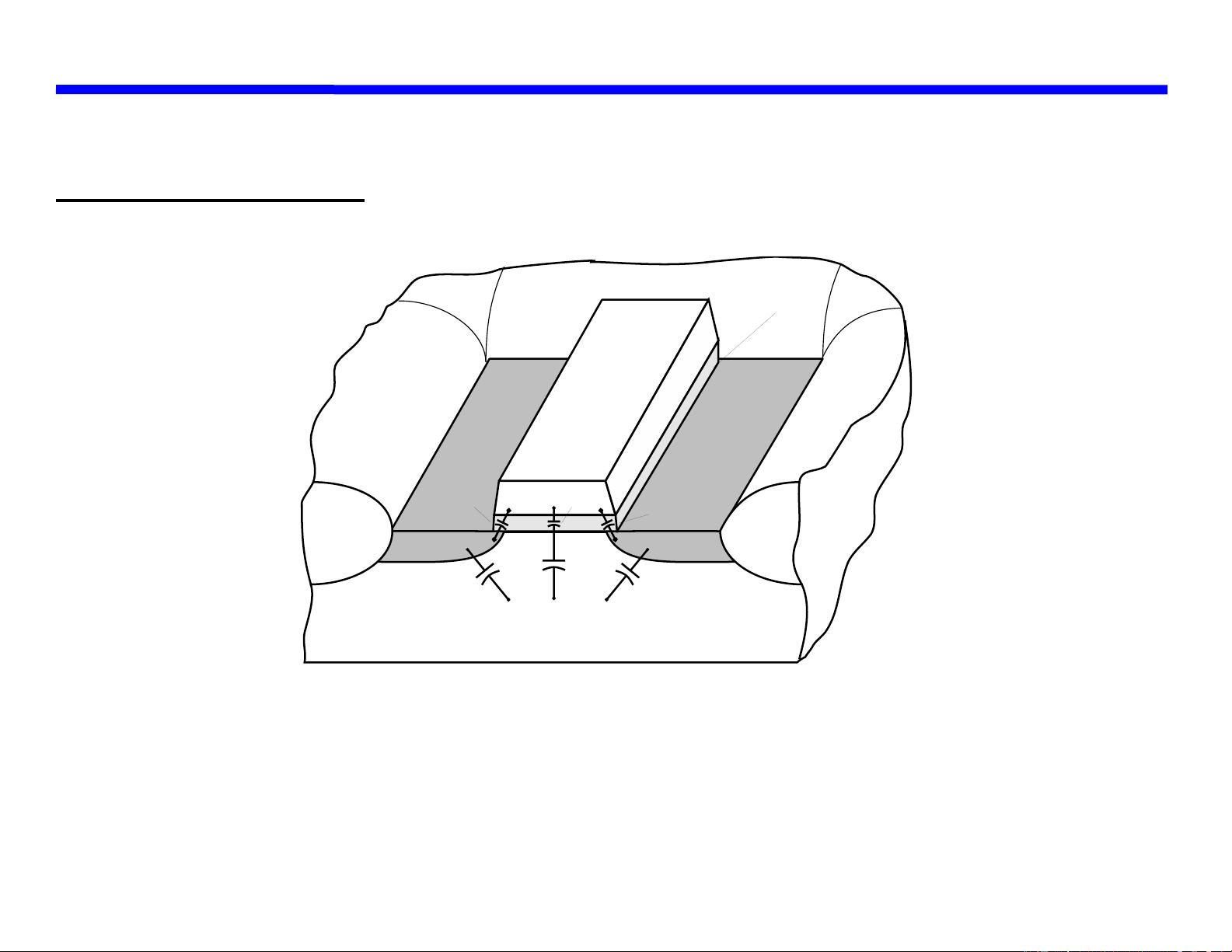
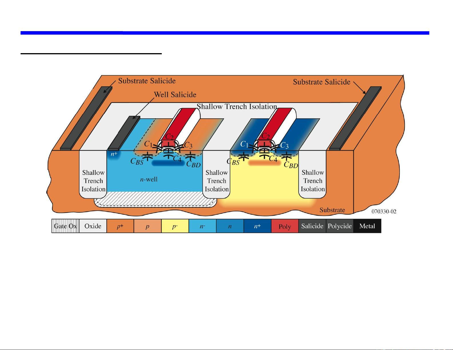
Use of Shallow Trench Isolation Technology
Shallow trench isolation (STI) allows closer spacing of transistors by eliminating the
depletion region at the surface.
p
+
pp
-
MetalSalicide
n
-
n n
+
Oxide
Poly
070330-03
Polycide
Gate Ox
n
+
n-well
n
+
p-well
n
+
Substrate
n
+
Shallow
Trench
Isolation
n
+
Shallow
Trench
Isolation
Shallow
Trench
Isolation
p
+
p
+
n
+
n
+
Substrate Salicide
Well Salicide
Decreased
spacing
Substrate Salicide
S
h
a
l
l
o
w
Trench Isolation
I
s
o
l
a
t
i
o
n
S
h
a
l
l
o
w
T
r
e
n
c
h
Lecture 03 – DSM CMOS Technology (11/16/15) Page 03-4
CMOS Analog Circuit Design © P.E. Allen - 2016
Comparison of STI and LOCOS
What are the differences between a LOCOS and STI technology?
Comments:
• If the n
+
to p
+
spacing is large, the Bird’s beak can be compensated using techniques
such as poly buffered LOCOS
• At some point as the n
+
to p
+
spacing gets smaller, the restricted bird’s beak leads to
undesirable stress effects in the transistor.
• An important advantage of STI is that it minimizes the heat cycle needed for n
+
or p
+
isolation compared to LOCOS. This is a significant advantage for any process where
there are implants before STI.
Lecture 03 – DSM CMOS Technology (11/16/15) Page 03-5
CMOS Analog Circuit Design © P.E. Allen - 2016
Shallow Trench Isolation (STI)
060203-01
Nitride
Silicon
(1)
(2)
(3)
(4)
(5)
(6)
1.) Cover the wafer with pad oxide and silicon nitride.
2.) First etch nitride and pad oxide. Next, an anisotropic
etch is made in the silicon to a depth of 0.4 to 0.5 microns.
3.) Grow a thin thermal oxide layer on the trench walls.
4.) A CVD dielectric film is used to fill the trench.
5.) A chemical mechanical polishing (CMP) step is used to
polish back the dielectric layer until the nitride is reached.
The nitride acts like a CMP stop layer.
6.) Densify the dielectric material at 900°C and strip the
nitride and pad oxide.


评论0