没有合适的资源?快使用搜索试试~ 我知道了~
ADC/DAC应用设计宝典,比较值得一看
资源详情
资源评论
资源推荐
ABCs of ADCs - Rev 3, June 2006
Authored by: Nicholas “Nick” Gray
Copyright 2003, 2004, 2006 National Semiconductor
Corporation
All rights reserved
1
ABCs of ADCs
Analog-to-Digital Converter Basics
Nicholas Gray
Data Conversion Systems
Staff Applications Engineer
November 24, 2003
Corrected August 13, 2004
Additional Corrections June 27, 2006
ABCs of ADCs - Rev 3, June 2006
Authored by: Nicholas “Nick” Gray
Copyright 2003, 2004, 2006 National Semiconductor
Corporation
All rights reserved
2
2
Agenda - ABCs of ADCs
• What’s an ADC?
• Review of Definitions
• Sources of Distortion and Noise
• Common Design Mistakes
• High Speed ADCs at National
ABCs of ADCs - Rev 3, June 2006
Authored by: Nicholas “Nick” Gray
Copyright 2003, 2004, 2006 National Semiconductor
Corporation
All rights reserved
3
3
October 2001
What Is an ADC?
• Mixed-Signal Device
– Analog Input
– Digital Output
• May be Considered to be a Divider
– Output says: Input is What Fraction of V
REF
?
– Output = 2
n
x G x A
IN
/ V
REF
• n = # of Output Bits (Resolution)
• G = Gain Factor (usually “1”)
• A
IN
= Analog Input Voltage (or Current)
• V
REF
(I
REF
)= Reference Voltage (or Current)
Because the Analog-to-Digital Converter (A/D Converter or ADC) has both analog and digital
functions, it is a mixed-signal device. Many of us consider the ADC to be a mysterious device.
It can, however, be considered very simply to be the instrument that it is: a device that
provides an output that digitally represents the input voltage or current level.
Notice I said voltage or current. Most ADCs convert an input voltage to a digital word, but the
true definition of an ADC does include the possibility of an input current.
An ADC has an analog reference voltage or current against which the analog input is
compared. The digital output word tells us what fraction of the reference voltage or current is
the input voltage or current. So, basically, the ADC is a divider.
The Input/Output transfer function is given by the formula indicated here. If you have seen this
formula before, you probably did not see the “G” term (gain factor). This is because we
generally consider this to be unity. However, National Semiconductor has introduced ADCs
with other gain factors, so it is important to understand that this factor is present.
___________________________________________________________________________
_
PLEASE NOTE: The discussion here assumes an ADC with a binary output. Some of the
statements here would be modified slightly for Offset Binary or 2’s Complement outputs.
ABCs of ADCs - Rev 3, June 2006
Authored by: Nicholas “Nick” Gray
Copyright 2003, 2004, 2006 National Semiconductor
Corporation
All rights reserved
4
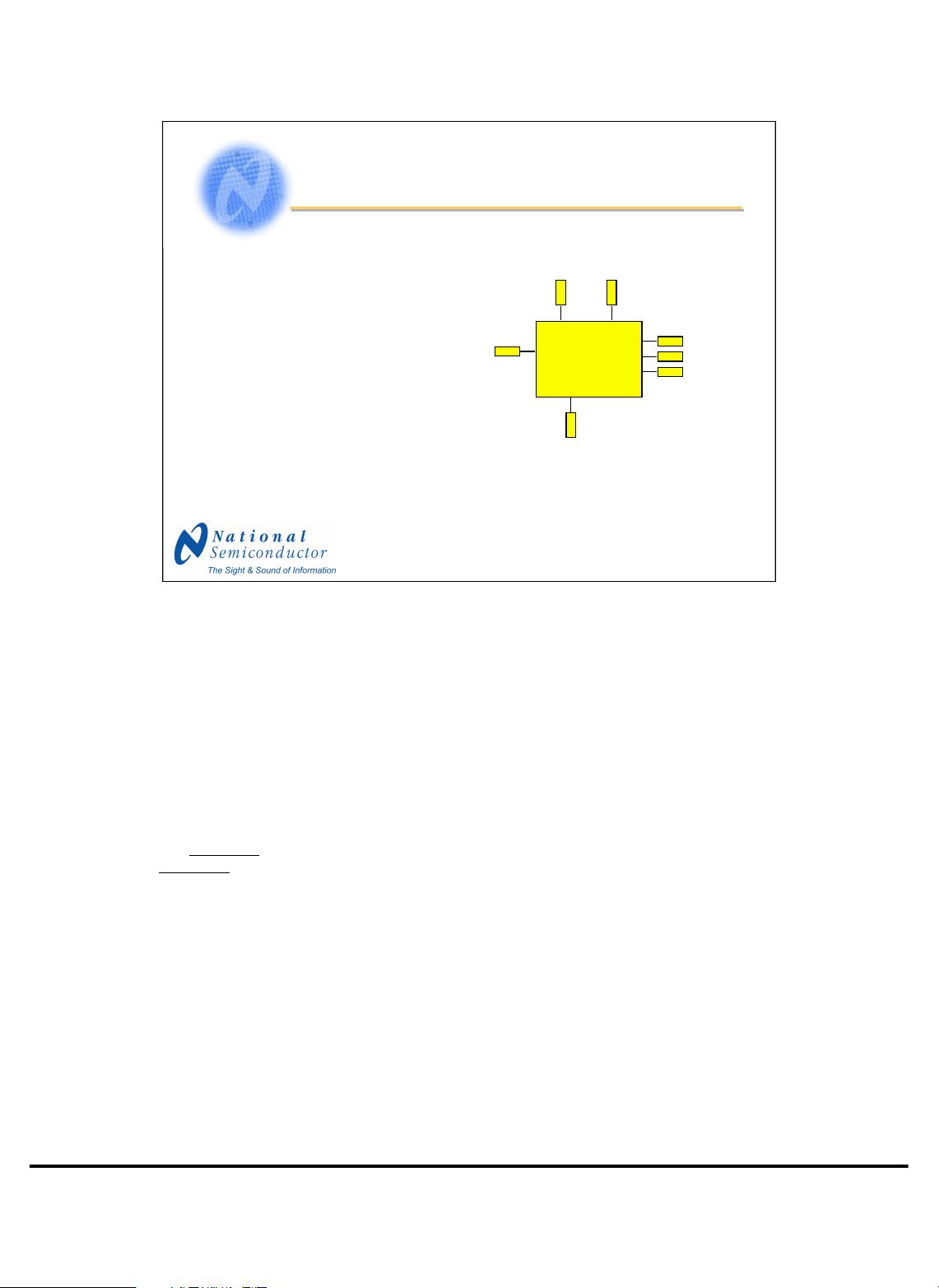
Here is an example of a 3-bit A/D converter. Because it has 3 bits, there are 2
3
= 8 possible
output codes. The difference between each output code is V
REF
/ 2
3
.
Assuming that the output response has no errors, every time you increase the voltage at the
input by 1 Volt, the output code will increase by one bit. This means, in this example, that the
least significant bit (LSB) represents 1 Volt, which is the smallest increment that this converter
can resolve. For this reason, we can say that the resolution of this converter is 1.0V because
we can resolve voltages as small as a volt. Resolution may also be stated in bits.
Note that if you reduce the reference voltage to 0.8V, the LSB would then represent 100mV,
allowing you to measure a smaller range of voltages (0 to 0.8V) with greater accuracy. This is
a common way for our customers to get better precision from a converter without buying a
more expensive, higher resolution converter.
The Resolution
of an A/D converter is the number of output bits it has (3 bits, in this example).
Resolution
may also be defined as the size of the LSB (Least Significant Bit) or one count (1
Volt, in this example).
4
What, Exactly, Does An Analog-
to-Digital Converter Do?
• For a 3-bit ADC, there are 8
possible output codes.
• In this example, if the input
voltage is 5.5V and the
reference is 8V, then the
output will be 101.
• More bits give better
resolution and smaller steps.
• A lower reference voltage
gives smaller steps, but can
be at the expense of noise.
A/D
Converter
Analog
Input
0V < 000 < 1V
1V < 001 < 2V
2V < 010 < 3V
3V < 011 < 4V
4V < 100 < 5V
5V < 101 < 6V
6V < 110 < 7V
7V < 111 < 8V
+V
CC
V
REF
(8V)
GND
ABCs of ADCs - Rev 3, June 2006
Authored by: Nicholas “Nick” Gray
Copyright 2003, 2004, 2006 National Semiconductor
Corporation
All rights reserved
5
The Least and Most Significant Bits (LSB and MSB) are just what their name implies: those
bits that have the least weight (LSB) and most weight (MSB) in a digital word. For an n-bit
word, the MSB has a weight of 2
(n-1)
= 2
n
/ 2 where “n” is the total number of bits in the word.
The LSB has a weight of 1.
5
Least Significant Bit (LSB)
and
Most Significant Bit (MSB)
NCG 9/99
B7 B6 B5 B4 B3 B2 B1 B0
Bit Weights of an 8-Bit Word
MSB LSB
128 64 32 16 8 4 2 1
0 1 1 0 0 1 0 . . . 0
Weight
Least Significant Bit 2
(n-?)
7th Most Significant Bit 2
(n-7)
6th Most Significant Bit 2
(n-6)
5th Most Significant Bit 2
(n-5)
4th Most Significant Bit 2
(n-4)
3rd Most Significant Bit 2
(n-3)
2nd Most Significant Bit 2
(n-2)
Most Significant Bit 2
(n-1)
剩余63页未读,继续阅读
121lllllll
- 粉丝: 0
- 资源: 1
上传资源 快速赚钱
- 我的内容管理 展开
- 我的资源 快来上传第一个资源
- 我的收益 登录查看自己的收益
- 我的积分 登录查看自己的积分
- 我的C币 登录后查看C币余额
- 我的收藏
- 我的下载
- 下载帮助
安全验证
文档复制为VIP权益,开通VIP直接复制
信息提交成功
评论0