没有合适的资源?快使用搜索试试~ 我知道了~
VTI7064MSME_SPI的RAM芯片手册.PDF
需积分: 47 27 下载量 31 浏览量
2019-05-23
09:14:01
上传
评论 1
收藏 2.81MB PDF 举报
温馨提示
试读
13页
vti7064,SPI接口的的RAM存储器芯片文档,适合需要暂存大量数据的,脚位要求少的应用
资源推荐
资源详情
资源评论
1
VTI7064xxxxx
64MbitSerialSRAM
Vilsion Technology Inc.
Rev.0.1,1/2017
Document Title
64Mbit Serial SRAM Specification
Revision History
Revision No. History Date Remark
0.1 Initial Draft March. 31 2017 Preliminary
2
VTI7064xxxxx
64MbitSerialSRAM
Vilsion Technology Inc.
Rev.0.1,1/2017
1.General Description
This document defines “64Mbit Serial SRAM”, which support 1.8v & 3.0V 64Mbit of SPI/QPI (Serial Peripheral
Interface/Quad Peripheral Interface) SRAM device. This RAM is configurable as 1 bit Input and Output separate or 4
bit I/O common interface. All of necessary Refresh operation is taken care by device itself.
Features
-SPI Bus Interface:
SPI compatible
SQI(qual) compatible
20 MHz Clock rate for all mode
-Low-Power CMOS Technology:
Read Current: Max.25mA
Standby Current: Typical 50uA
-Unlimited Read and Write Cycles
-8M x 8-bit Organization & 1Kbytes page size
-High Reliability
-RoHS Compliant
-8 Lead SOIC Package
-Temperature Ranges Supported:
Extended(E): -25°C to +85°C
Industrial(I): -40°C to +85°C
Product Family
Part Number Temperature Ranges Power Supply Packages
VTI7064LSME E 1.6V~2.0V 8pin SOIC
VTI7064LSMI I 1.6V~2.0V 8pin SOIC
VTI7064MSME E 2.7V~3.3V 8pin SOIC
VTI7064MSMI I 2.7V~3.3V 8pin SOIC
2.Pin Description
8pin SOIC 150mil
#CE
SO/SIO1
SIO2
V
SS
SIO3
V
DD
SCLK
SI/SIO0
3
VTI7064xxxxx
64MbitSerialSRAM
Vilsion Technology Inc.
Rev.0.1,1/2017
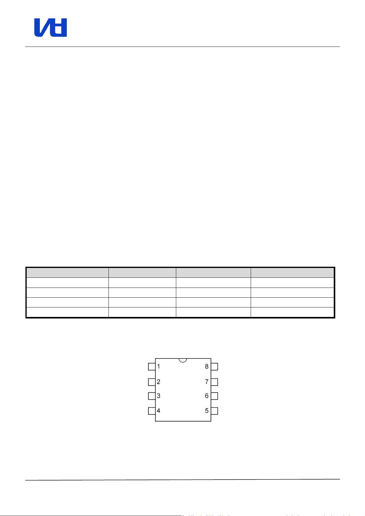
Symbol Signal Type SPI Mode QPI Mode
V
DD
Power Core Power Supply
V
SS
Ground Core Supply Ground
CE# Input
Chip select signal, Active Low. When CE# input isHigh, memory will be in
Standby state
CLK Input Clock Signal
SI/SIO[0] I/O Serial Input I/O[0]
SO/SIO[1] I/O Serial Output I/O[1]
SIO[3:2] I/O I/O[3:2]
1
I/O[3:2]
Note:1,Fast read Quad access and Quad Write access in SPI Mode use SIO[3:2].Recommend to pull down to GND if no use of SIO[3:2] in SPI
mode.
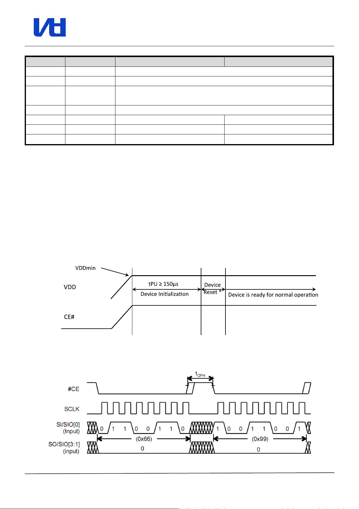
3. Power up initialization
All products include an on−chip voltage sensor used to start the self−initialization process. When V
DD
reaches a
stable level at or above minimum V
DD
, the device will require 150μs to complete its self−initialization process. From
the beginning of power ramp to the end of the 150μs period, CLK should remain LOW, CE# should remain HIGH
(track V
DD
within 200mV) and SI/SO/SIO[3:0] should remain LOW.
After the 150us period the device requires initialization command sequence as it’s shown in Figure 2, and then the
device is ready for normal operation.
Figure 1. Power-Up Initialization Timing
Figure 2. Reset command sequence for Device Initialization
剩余12页未读,继续阅读
资源评论
布丁electronics
- 粉丝: 5
- 资源: 2
上传资源 快速赚钱
- 我的内容管理 展开
- 我的资源 快来上传第一个资源
- 我的收益 登录查看自己的收益
- 我的积分 登录查看自己的积分
- 我的C币 登录后查看C币余额
- 我的收藏
- 我的下载
- 下载帮助
安全验证
文档复制为VIP权益,开通VIP直接复制
信息提交成功