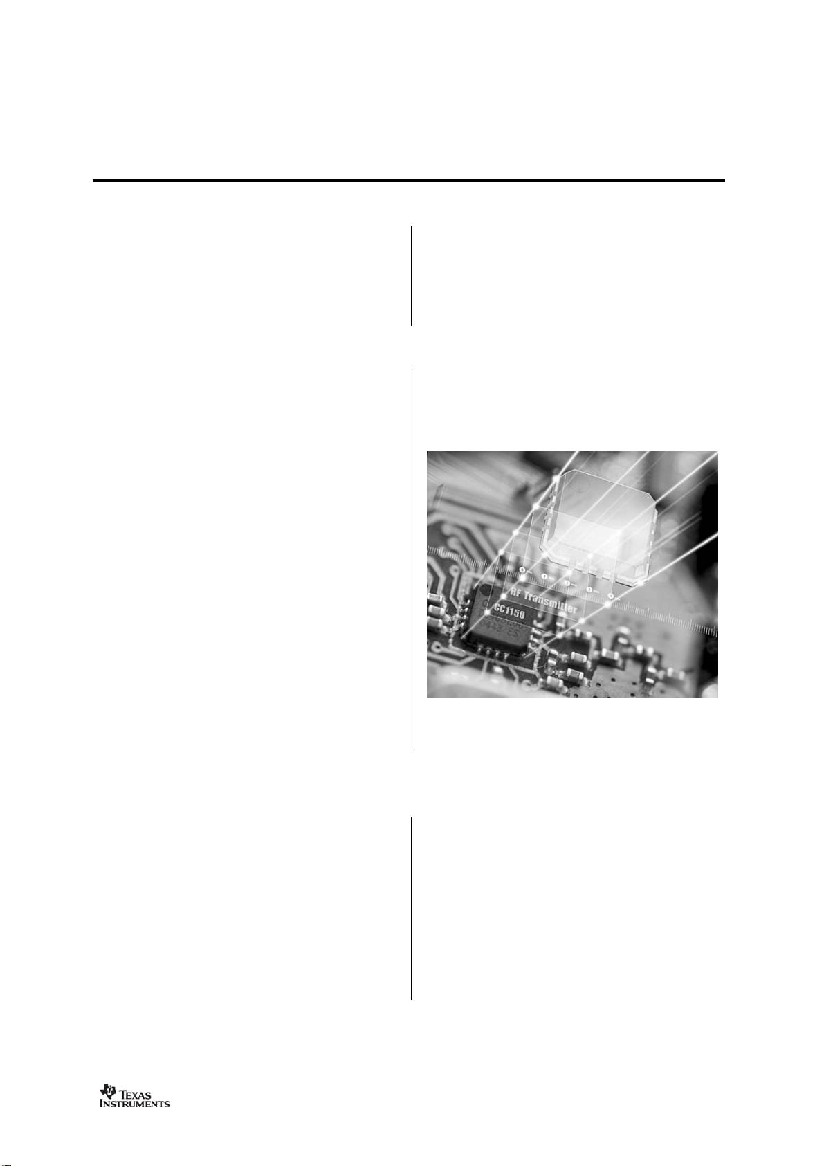
没有合适的资源?快使用搜索试试~ 我知道了~
这是一款无线接收和发射于一体的RF IC,属于微功率无线电领域.
资源详情
资源评论
资源推荐
CC1150
SWRS037A Page 1 of 60
CC1150
Low Power Sub-1 GHz RF Transmitter
Applications
• Ultra low power UHF wireless transmitters
• Operating in the 315/433/868/915 MHz
ISM/SRD bands
• AMR – Automatic Meter Reading
• Consumer Electronics
• RKE – Remote Keyless Entry
• Low power telemetry
• Home and building automation
• Wireless alarm and security systems
• Industrial monitoring and control
• Wireless sensor networks
Product Description
The
CC1150
is a low cost true single chip UHF
transmitter designed for very low power
wireless applications. The circuit is mainly
intended for the ISM (Industrial, Scientific and
Medical) and SRD (Short Range Device)
frequency bands at 315, 433, 868 and 915
MHz, but can easily be programmed for
operation at other frequencies in the 300-348
MHz, 400-464 MHz and 800-928 MHz bands.
The RF transmitter is integrated with a highly
configurable baseband modulator. The
modulator supports various modulation
formats and has a configurable data rate up to
500 kBaud. The
CC1150
provides extensive
hardware support for packet handling, data
buffering and burst transmissions.
The main operating parameters and the 64-
byte transmit FIFO of
CC1150
can be controlled
via an SPI interface. In a typical system, the
CC1150
will be used together with a micro-
controller and a few additional passive
components.
CC1150
is part of Chipcon’s SmartRF®04
technology platform based on 0.18 µm CMOS
technology.
Key Features
• Small size (QLP 4x4 mm package, 16
pins)
• True single chip UHF RF transmitter
• Frequency bands: 300-348 MHz, 400-464
MHz and 800-928 MHz
• Programmable data rate up to 500 kBaud
• Low current consumption
• Programmable output power up to +10
dBm for all supported frequencies
• Programmable baseband modulator
• Ideal for multi-channel operation
• Very few external components:
Completely on-chip frequency synthesizer,
no external filters needed
• Configurable packet handling hardware
• Suitable for frequency hopping systems
due to a fast settling frequency synthesizer
• Optional Forward Error Correction with
interleaving
• 64-byte TX data FIFO
CC1150
SWRS037A Page 2 of 60
Features (continued from front page)
• Suited for systems compliant with EN 300
220 and FCC CFR Part 15
• Many powerful digital features allow a
high-performance RF system to be made
using an inexpensive microcontroller
• Efficient SPI interface: All registers can be
programmed with one “burst” transfer
• Integrated analog temperature sensor
• Lead-free “green” package
• Flexible support for packet oriented
systems: On chip support for sync word
insertion, flexible packet length and
automatic CRC handling
• OOK and flexible ASK shaping supported
• 2-FSK, GFSK and MSK supported
• Optional automatic whitening of data
• Support for asynchronous transparent
transmit mode for backwards compatibility
with existing radio communication
protocols
Abbreviations
Abbreviations used in this data sheet are described below.
ADC Analog to Digital Converter NRZ Non Return to Zero (Coding)
AFC Automatic Frequency Compensation OOK On-Off-Keying
AGC Automatic Gain Control PA Power Amplifier
AMR Automatic Meter Reading PCB Printed Circuit Board
ASK Amplitude Shift Keying PD Power Down
BER Bit Error Rate PER Packet Error Rate
CCA Clear Channel Assessment PLL Phase Locked Loop
CFR Code of Federal Regulations POR Power-On Reset
CRC Cyclic Redundancy Check QLP Quad Leadless Package
CW Contionus Wave (Unmodulated Carrier) QPSK Quadrature Phase Shift Keying
DC Direct Current RC Resistor-Capacitor
EIRP Equivalent Isotropic Radiated Power RCOSC RC Oscillator
ESR Equivalent Series Resistance RF Radio Frequency
FCC Federal Communications Commission RSSI Received Signal Strength Indicator
FEC Forward Error Correction RX Receive, Receive Mode
FIFO First-In-First-Out SAW Surface Aqustic Wave
FSK Frequency Shift Keying SMD Surface Mount Device
GFSK Gaussian shaped Frequency Shift Keying SNR Signal to Noise Ratio
ISM Industrial, Scientific, Medical SPI Serial Peripheral Interface
LC Inductor-Capacitor SRD Short Range Devices
LO Local Oscillator TBD To Be Defined
LSB Least Significant Byte TX Transmit, Transmit Mode
LQI Link Quality Indicator UHF Ultra High frequency
MCU Microcontroller Unit VCO Voltage Controlled Oscillator
MSK Minimum Shift Keying XOSC Crystal Oscillator
N/A Not Applicable XTAL Crystal
CC1150
SWRS037A Page 3 of 60
Table Of Contents
APPLICATIONS...........................................................................................................................................1
PRODUCT DESCRIPTION.........................................................................................................................1
KEY FEATURES..........................................................................................................................................1
FEATURES (CONTINUED FROM FRONT PAGE)................................................................................2
ABBREVIATIONS...............................................................................................................................................2
TABLE OF CONTENTS..............................................................................................................................3
1 ABSOLUTE MAXIMUM RATINGS...........................................................................................................5
2 OPERATING CONDITIONS......................................................................................................................5
3 GENERAL CHARACTERISTICS ...............................................................................................................5
4 ELECTRICAL SPECIFICATIONS...............................................................................................................6
4.1 CURRENT CONSUMPTION .....................................................................................................................6
4.2 RF TRANSMIT SECTION ........................................................................................................................7
4.3 CRYSTAL OSCILLATOR.........................................................................................................................8
4.4 FREQUENCY SYNTHESIZER CHARACTERISTICS.....................................................................................8
4.5 ANALOG TEMPERATURE SENSOR .........................................................................................................9
4.6 DC CHARACTERISTICS .........................................................................................................................9
4.7 POWER ON RESET .................................................................................................................................9
5 PIN CONFIGURATION..........................................................................................................................10
6 CIRCUIT DESCRIPTION........................................................................................................................11
7 APPLICATION CIRCUIT........................................................................................................................11
7.1 BIAS RESISTOR ...................................................................................................................................11
7.2 BALUN AND RF MATCHING ................................................................................................................11
7.3 CRYSTAL ............................................................................................................................................12
7.4 REFERENCE SIGNAL............................................................................................................................12
7.5 ADDITIONAL FILTERING......................................................................................................................12
7.6 POWER SUPPLY DECOUPLING..............................................................................................................12
7.7 ANTENNA CONSIDERATIONS ..............................................................................................................13
7.8 PCB LAYOUT RECOMMENDATIONS....................................................................................................15
8 CONFIGURATION OVERVIEW ..............................................................................................................16
9 CONFIGURATION SOFTWARE ..............................................................................................................17
10 4-WIRE SERIAL CONFIGURATION AND DATA INTERFACE ...................................................................18
10.1 CHIP STATUS BYTE ............................................................................................................................19
10.2 REGISTER ACCESS ..............................................................................................................................20
10.3 SPI READ ...........................................................................................................................................20
10.4 COMMAND STROBES ..........................................................................................................................20
10.5 FIFO ACCESS.....................................................................................................................................21
10.6 PATABLE ACCESS............................................................................................................................22
11 MICROCONTROLLER INTERFACE AND PIN CONFIGURATION...............................................................22
11.1 CONFIGURATION INTERFACE..............................................................................................................22
11.2 GENERAL CONTROL AND STATUS PINS ..............................................................................................22
11.3 OPTIONAL RADIO CONTROL FEATURE ...............................................................................................23
12 DATA RATE PROGRAMMING...............................................................................................................23
13 PACKET HANDLING HARDWARE SUPPORT .........................................................................................24
13.1 DATA WHITENING...............................................................................................................................24
13.2 PACKET FORMAT................................................................................................................................25
13.3 PACKET HANDLING IN TRANSMIT MODE............................................................................................26
13.4 PACKET HANDLING IN FIRMWARE......................................................................................................26
14 MODULATION FORMATS.....................................................................................................................27
14.1 FREQUENCY SHIFT KEYING ................................................................................................................27
14.2 MINIMUM SHIFT KEYING....................................................................................................................27
14.3 AMPLITUDE MODULATION .................................................................................................................28
15 FORWARD ERROR CORRECTION WITH INTERLEAVING........................................................................28
15.1 FORWARD ERROR CORRECTION (FEC)...............................................................................................28
15.2 INTERLEAVING ...................................................................................................................................28
CC1150
SWRS037A Page 4 of 60
16 RADIO CONTROL ................................................................................................................................30
16.1 POWER ON START-UP SEQUENCE........................................................................................................31
16.2 CRYSTAL CONTROL............................................................................................................................31
16.3 VOLTAGE REGULATOR CONTROL.......................................................................................................32
16.4 ACTIVE MODE....................................................................................................................................32
16.5 TIMING ...............................................................................................................................................32
17 DATA FIFO ........................................................................................................................................33
18 FREQUENCY PROGRAMMING ..............................................................................................................34
19 VCO...................................................................................................................................................34
19.1 VCO AND PLL SELF-CALIBRATION ...................................................................................................34
20 VOLTAGE REGULATORS .....................................................................................................................35
21 OUTPUT POWER PROGRAMMING ........................................................................................................35
21.1 SHAPING AND PA RAMPING ...............................................................................................................36
22 GENERAL PURPOSE / TEST OUTPUT CONTROL PINS ...........................................................................37
23 ASYNCHRONOUS AND SYNCHRONOUS SERIAL OPERATION ................................................................39
23.1 ASYNCHRONOUS SERIAL OPERATION.................................................................................................39
23.2 SYNCHRONOUS SERIAL OPERATION ...................................................................................................39
24 SYSTEM CONSIDERATIONS AND GUIDELINES......................................................................................39
24.1 SRD REGULATIONS............................................................................................................................39
24.2 FREQUENCY HOPPING AND MULTI-CHANNEL SYSTEMS.....................................................................40
24.3 WIDEBAND MODULATION NOT USING SPREAD SPECTRUM.................................................................40
24.4 DATA BURST TRANSMISSIONS............................................................................................................41
24.5 CONTINUOUS TRANSMISSIONS ...........................................................................................................41
24.6 LOW COST SYSTEMS ..........................................................................................................................41
24.7 BATTERY OPERATED SYSTEMS ..........................................................................................................41
24.8 INCREASING OUTPUT POWER .............................................................................................................41
25 CONFIGURATION REGISTERS ..............................................................................................................42
25.1 CONFIGURATION REGISTER DETAILS .................................................................................................45
25.2 STATUS REGISTER DETAILS.................................................................................................................55
26 PACKAGE DESCRIPTION (QLP 16)......................................................................................................57
26.1 RECOMMENDED PCB LAYOUT FOR PACKAGE (QLP 16).....................................................................57
26.2 SOLDERING INFORMATION..................................................................................................................57
27 REFERENCES.......................................................................................................................................58
28 GENERAL INFORMATION ....................................................................................................................59
28.1 DOCUMENT HISTORY .........................................................................................................................59
CC1150
SWRS037A Page 5 of 60
1 Absolute Maximum Ratings
Under no circumstances must the absolute maximum ratings given in Table 1 be violated. Stress
exceeding one or more of the limiting values may cause permanent damage to the device.
Caution! ESD sensitive device.
Precaution should be used when handling
the device in order to prevent permanent
damage.
Parameter Min Max Units Condition
Supply voltage –0.3 3.6 V All supply pins must have the same voltage
Voltage on any digital pin –0.3 VDD+0.3
max 3.6
V
Voltage on the pins RF_P, RF_N
and DCOUPL
–0.3 2.0 V
Voltage ramp-up 120 kV/µs
Input RF level +10 dBm
Storage temperature range –50 150
°C
Solder reflow temperature 260
°C
According to IPC/JEDEC J-STD-020C
ESD <500 V According to JEDEC STD 22, method A114,
Human Body Model
Table 1: Absolute Maximum Ratings
2 Operating Conditions
The operating conditions for
CC1150
are listed Table 2 in below.
Parameter Min Max Unit Condition
Operating temperature -40 85
°C
Operating supply voltage 1.8 3.6 V All supply pins must have the same voltage
Table 2: Operating Conditions
3 General Characteristics
Parameter Min Typ Max Unit Condition/Note
300 348 MHz
400 464 MHz
Frequency range
800 928 MHz
Data rate 1.2
1.2
26
500
250
500
kBaud
kBaud
kBaud
2-FSK
GFSK, OOK and ASK
(Shaped) MSK (also known as differential offset
QPSK)
Optional Manchester encoding (the data rate in kbps
will be half the baud rate)
Table 3: General Characteristics
剩余60页未读,继续阅读
ma94938
- 粉丝: 0
- 资源: 5
上传资源 快速赚钱
- 我的内容管理 展开
- 我的资源 快来上传第一个资源
- 我的收益 登录查看自己的收益
- 我的积分 登录查看自己的积分
- 我的C币 登录后查看C币余额
- 我的收藏
- 我的下载
- 下载帮助
最新资源
- 第十四届中北大学ACM程序设计竞赛.zip
- UIGF_200852355_202404242026.json
- 基于深度学习的对话系统、语音识别、机器翻译和语音合成等
- 基于STM32单片机的智能停车场设计源码+全部资料.zip
- 534springboot + vue 实验室管理系统.zip(可运行源码+数据库文件+文档)
- 基于Python+Opencv+keras的实时手势识别系统+源码+文档(期末大作业&课程设计&项目开发)
- 基于Python+joint-spider爬虫数据的成都二手房数据分析源码+详细使用说明.zip
- 基于YOLOv7-plate和CRNN的车牌号检测识别项目,使用PyQt构建了UI界面
- 基于LabView+MATLAB的说话人识别系统.zip
- 基于树莓派+OpenCV+Python语言的人脸识别+源码+开发文档(毕业设计&课程设计&项目开发)
资源上传下载、课程学习等过程中有任何疑问或建议,欢迎提出宝贵意见哦~我们会及时处理!
点击此处反馈
安全验证
文档复制为VIP权益,开通VIP直接复制
信息提交成功
评论0