


Sitronix Technology Corp. reserves the right to change the contents in this
document without prior notice.
ST7735S
132RGB x 162dot 262K Color with Frame Memory
Single-Chip TFT Controller/Driver
Datasheet
Version 1.5
2015/ 3
ST7735S
V 1.5 Page 2 of 201 2015- 3- 3
LIST OF CONTENT
1 GENERAL DESCRIPTION ......................................................................10
2 FEATURES ..............................................................................................10
3 PAD ARRANGEMENT ............................................................................12
3.1 Output Bump Dimension........................................................................................12
3.2 Input Bump Dimension...........................................................................................13
3.3 Alignment Mark Dimension ....................................................................................14
3.4 Chip Information.....................................................................................................15
4 PAD CENTER COORDINATES ..............................................................16
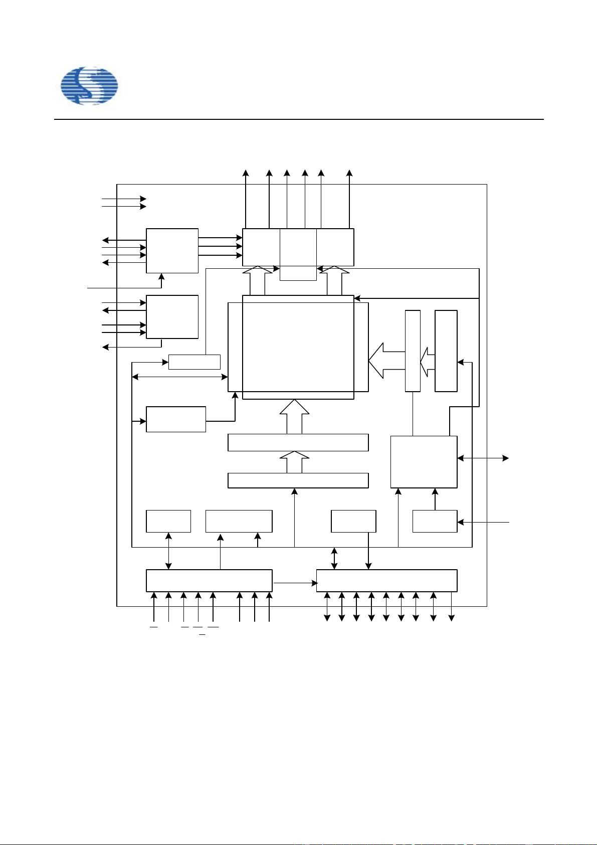
5 BLOCK DIAGRAM ..................................................................................22
6 PIN DESCRIPTION..................................................................................23
6.1 Power Supply Pin...................................................................................................23
6.2 Interface Logic Pin .................................................................................................23
6.3 Mode Selection Pin ................................................................................................25
6.4 Driver Output pins..................................................................................................26
6.5 Test Pins................................................................................................................27
7 DRIVER ELECTRICAL CHARACTERISTICS ........................................28
7.1 Absolute Operation Range.....................................................................................28
7.2 DC Characteristic...................................................................................................29
7.3 Power Consumption...............................................................................................30
8 Timing chart............................................................................................31
8.1 Parallel Interface Characteristics: 18, 16, 9 or 8-bit Bus (8080 Series MCU Interface)
31
8.2 Parallel Interface Characteristics: 18, 16, 9 or 8-bit Bus (6800 Series MCU Interface)
33
8.3 Serial Interface Characteristics (3-line Serial)........................................................35
8.4 Serial Interface Characteristics (4-line Serial)........................................................36
9 Function Description .............................................................................37
9.1 Interface Type Selection ........................................................................................37
9.2 8080-series MCU Parallel Interface (P68 = ‘0’)......................................................38
9.2.1 Write Cycle Sequence........................................................................................................39
9.2.2 Read Cycle Sequence..........................................................................................................40
9.3 6800-series MCU Parallel Interface (P68 = ‘1’)......................................................41
9.3.1 Write Cycle Sequence..........................................................................................................42
9.3.2 Read Cycle Sequence..........................................................................................................43
9.4 Serial Interface.......................................................................................................44
9.4.1 Command Write Mode..........................................................................................................44
9.4.2 Read Functions....................................................................................................................46
ST7735S
V 1.5 Page 3 of 201 2015- 3- 3
9.4.3 3-line Serial Protocol ............................................................................................................46
9.4.4 4-line Serial Protocol ............................................................................................................47
9.5 Data Transfer Break and Recovery........................................................................48
9.6 Data Transfer Pause..............................................................................................50
9.6.1 Serial Interface Pause ..........................................................................................................50
9.6.2 Parallel Interface Pause .......................................................................................................50
9.7 Data Transfer Modes .............................................................................................51
9.7.1 Method 1..............................................................................................................................51
9.7.2 Method 2..............................................................................................................................51
9.8 Data Color Coding .................................................................................................52
9.8.1 8-bit Parallel Interface (IM2, IM1, IM0= “100”).......................................................................52
9.8.2 8-bit Data Bus for 12-bit/Pixel (RGB 4-4-4-bit Input), 4K-Colors, 3AH= “03h”.........................52
9.8.3 8-bit Data Bus for 16-bit/Pixel (RGB 5-6-5-bit Input), 65K-Colors, 3AH= “05h”.......................53
9.8.4 8-bit Data Bus for 18-bit/Pixel (RGB 6-6-6-bit Input), 262K-Colors, 3AH= “06h”.....................54
9.8.5 16-Bit Parallel Interface (IM2,IM1, IM0= “101”)......................................................................55
9.8.6 16-bit Data Bus for 12-bit/Pixel (RGB 4-4-4-bit Input), 4K-Colors, 3AH= “03h”.......................55
9.8.7 16-bit Data Bus for 16-bit/Pixel (RGB 5-6-5-bit Input), 65K-Colors, 3AH= “05h”.....................56
9.8.8 16-bit Data Bus for 18-bit/Pixel (RGB 6-6-6-bit Input), 262K-Colors, 3AH= “06h”...................57
9.8.9 9-Bit Parallel Interface (IM2, IM1, IM0=“110”) .......................................................................58
9.8.10 Write 9-bit Data for RGB 6-6-6-bit Input (262k-color)...........................................................58
9.8.11 18-Bit Parallel Interface (IM2, IM1, IM0=“111”)....................................................................59
9.8.12 18-bit Data Bus for 12-bit/Pixel (RGB 4-4-4-bit Input), 4K-Colors, 3AH=“03h”......................59
9.8.13 18-bit Data Bus for 16-bit/Pixel (RGB 5-6-5-bit Input), 65K-Colors, 3AH=“05h”....................60
9.8.14 18-bit Data Bus for 18-bit/Pixel (RGB 6-6-6-bit Input), 262K-Colors, 3AH=“06h”..................61
9.8.15 3-line Serial Interface..........................................................................................................62
9.8.16 Write Data for 12-bit/Pixel (RGB 4-4-4-bit Input), 4K-Colors, 3AH=“03h” .............................62
9.8.17 Write Data for 16-bit/Pixel (RGB 5-6-5-bit Input), 65K-Colors, 3AH=“05h” ...........................63
9.8.18 Write Data for 18-bit/Pixel (RGB 6-6-6-bit Input), 262K-Colors, 3AH=“06h” .........................64
9.8.19 4-line Serial Interface..........................................................................................................65
9.8.20 Write Data for 12-bit/Pixel (RGB 4-4-4-bit Input), 4K-Colors, 3AH=“03h” .............................65
9.8.21 Write Data for 16-bit/Pixel (RGB 5-6-5-bit Input), 65K-Colors, 3AH=“05h” ...........................66
9.8.22 Write Data for 18-bit/Pixel (RGB 6-6-6-bit Input), 262K-Colors, 3AH=“06h” .........................66
9.9 Display Data RAM..................................................................................................67
9.9.1 Configuration (GM[1:0] = “00”)..............................................................................................67
9.9.2 Memory to Display Address Mapping....................................................................................68
9.9.3 When using 128RGB x 160 resolution (GM[1:0] = “11”, SMX=SMY=SRGB= ‘0’) ...................68
9.9.4 When using 132RGB x 132resolution (GM[1:0] = “01”, SMX=SMY=SRGB= ‘0’) ....................69
9.9.5 When using 132RGB x 162 resolution (GM[1:0] = “00”, SMX=SMY=SRGB= ‘0’) ...................70
ST7735S
V 1.5 Page 4 of 201 2015- 3- 3
9.9.6 Normal Display On or Partial Mode On .................................................................................71
9.9.7 When using 128RGB x 160 resolution (GM[1:0] = “11”) ........................................................71
9.9.8 When using 128RGB x 160 resolution (GM[1:0] = “01”) ........................................................72
9.9.9 When using 132RGB x 162 resolution (GM[1:0] = “00”) ........................................................73
9.10 Address Counter..................................................................................................74
9.11 Memory Data Write/ Read Direction ....................................................................75
9.11.1 When 128RGBx160 (GM= “11”) .........................................................................................75
9.11.2 When 132RGBx132 (GM= “01”) .........................................................................................75
9.11.3 When 132RGBx162 (GM= “00”) .........................................................................................76
9.11.4 Frame Data Write Direction According to the MADCTL Parameters (MV, MX and MY)........77
9.11.5 Scroll Address Circuit .........................................................................................................78
9.11.6 Vertical Scroll Mode ...........................................................................................................78
9.11.7 Vertical Scroll Example.......................................................................................................79
9.11.8 Case 1: TFA + VSA + BFA<162 .........................................................................................79
9.11.9 Case 2: TFA + VSA + BFA=162 (Rolling Scrolling) .............................................................80
9.12 Tearing Effect Output Line ...................................................................................81
9.12.1 Tearing Effect Line Modes..................................................................................................81
9.12.2 Tearing Effect Line Timings ................................................................................................82
9.12.3 Example 1: MPU Write is faster than panel read.................................................................83
9.12.4 Example 2: MPU Write is slower than panel read................................................................84
9.13 Power ON/OFF Sequence ...................................................................................85
9.13.1 Uncontrolled Power Off ......................................................................................................86
9.14 Power Level Definition .........................................................................................87
9.14.1 Power Level .......................................................................................................................87
9.14.2 Power Flow Chart...............................................................................................................88
9.15 Reset Table..........................................................................................................89
9.15.1 Reset Table(Default Value, GM[1:0]=“11”, 128RGB x 160) .................................................89
9.15.2 Reset Table (GM[1:0]= “01”, 132RGB x 132) ......................................................................90
9.15.3 Reset Table (GM[1:0]= “00”, 132RGB x 162) ......................................................................91
9.16 Module Input/Output Pins.....................................................................................92
9.16.1 Output or Bi-directional (I/O) Pins .......................................................................................92
9.17 Reset Timing........................................................................................................93
9.18 Color Depth Conversion Look Up Tables.............................................................94
9.18.1 65536 Color to 262,144 Color.............................................................................................94
9.18.2 4096 Color to 262,144 Color...............................................................................................98
9.19 Sleep Out-Command and Self-Diagnostic Functions of the Display Module......100
9.19.1 Register Loading Detection ..............................................................................................100
9.19.2 Functionality Detection .....................................................................................................101
ST7735S
V 1.5 Page 5 of 201 2015- 3- 3
9.19.3 Chip Attachment Detection (Optional)...............................................................................102
9.19.4 Display Glass Break Detection (Optional) .........................................................................103
10 COMMAND ............................................................................................104
10.1 System Function Command List and Description ..............................................104
10.1.1 NOP (00h)........................................................................................................................107
10.1.2 SWRESET (01h): Software Reset ....................................................................................108
10.1.3 RDDID (04h): Read Display ID .........................................................................................109
10.1.4 RDDST (09h): Read Display Status..................................................................................110
10.1.5 RDDPM (0Ah): Read Display Power Mode .......................................................................112
10.1.6 RDDMADCTL (0Bh): Read Display MADCTL ...................................................................113
10.1.7 RDDCOLMOD (0Ch): Read Display Pixel Format .............................................................114
10.1.8 RDDIM (0Dh): Read Display Image Mode ........................................................................115
10.1.9 RDDSM (0Eh): Read Display Signal Mode .......................................................................116
10.1.10 RDDSDR (0Fh): Read Display Self-Diagnostic Result.....................................................118
10.1.11 SLPIN (10h): Sleep In.....................................................................................................119
10.1.12 SLPOUT (11h): Sleep Out..............................................................................................120
10.1.13 PTLON (12h): Partial Display Mode On ..........................................................................121
10.1.14 NORON (13h): Normal Display Mode On........................................................................122
10.1.15 INVOFF (20h): Display Inversion Off...............................................................................123
10.1.16 INVON (21h): Display Inversion On ................................................................................124
10.1.17 GAMSET (26h): Gamma Set ..........................................................................................125
10.1.18 DISPOFF (28h): Display Off ...........................................................................................126
10.1.19 DISPON (29h): Display On .............................................................................................127
10.1.20 CASET (2Ah): Column Address Set................................................................................128
10.1.21 RASET (2Bh): Row Address Set.....................................................................................130
10.1.22 RAMWR (2Ch): Memory Write........................................................................................132
10.1.23 RGBSET (2Dh): Color Setting for 4K, 65K and 262K ......................................................133
10.1.24 RAMRD (2Eh): Memory Read ........................................................................................134
10.1.25 PTLAR (30h): Partial Area ..............................................................................................135
10.1.26 SCRLAR (33h): Scroll Area Set ......................................................................................137
10.1.27 TEOFF (34h): Tearing Effect Line OFF...........................................................................139
10.1.28 TEON (35h): Tearing Effect Line ON ..............................................................................140
10.1.29 MADCTL (36h): Memory Data Access Control ................................................................142
10.1.30 VSCSAD: Vertical Scroll Start Address of RAM (37h) .....................................................145
10.1.31 IDMOFF (38h): Idle Mode Off .........................................................................................147
10.1.32 IDMON (39h): Idle Mode On ...........................................................................................148
10.1.33 COLMOD (3Ah): Interface Pixel Format..........................................................................150
10.1.34 RDID1 (DAh): Read ID1 Value........................................................................................151


