基于spartan-3的PCI-E卡原理图
需积分: 10 115 浏览量
2012-09-05
21:32:47
上传
评论
收藏 498KB PDF 举报

5
5
4
4
3
3
2
2
1
1
D D
C C
B B
A A
Title
Size Document Number Rev
Date: Sheet of
Avnet, Inc.
Engineering Services
Copyright 2006
AES-SP3-PCIE-SCH 2.1
Spartan-3 PCIe Starter Board
B
1Thursday, May 03, 2007 13
Cover sheet
Title
Size Document Number Rev
Date: Sheet of
Avnet, Inc.
Engineering Services
Copyright 2006
AES-SP3-PCIE-SCH 2.1
Spartan-3 PCIe Starter Board
B
1Thursday, May 03, 2007 13
Cover sheet
Title
Size Document Number Rev
Date: Sheet of
Avnet, Inc.
Engineering Services
Copyright 2006
AES-SP3-PCIE-SCH 2.1
Spartan-3 PCIe Starter Board
B
1Thursday, May 03, 2007 13
Cover sheet
05/03/07
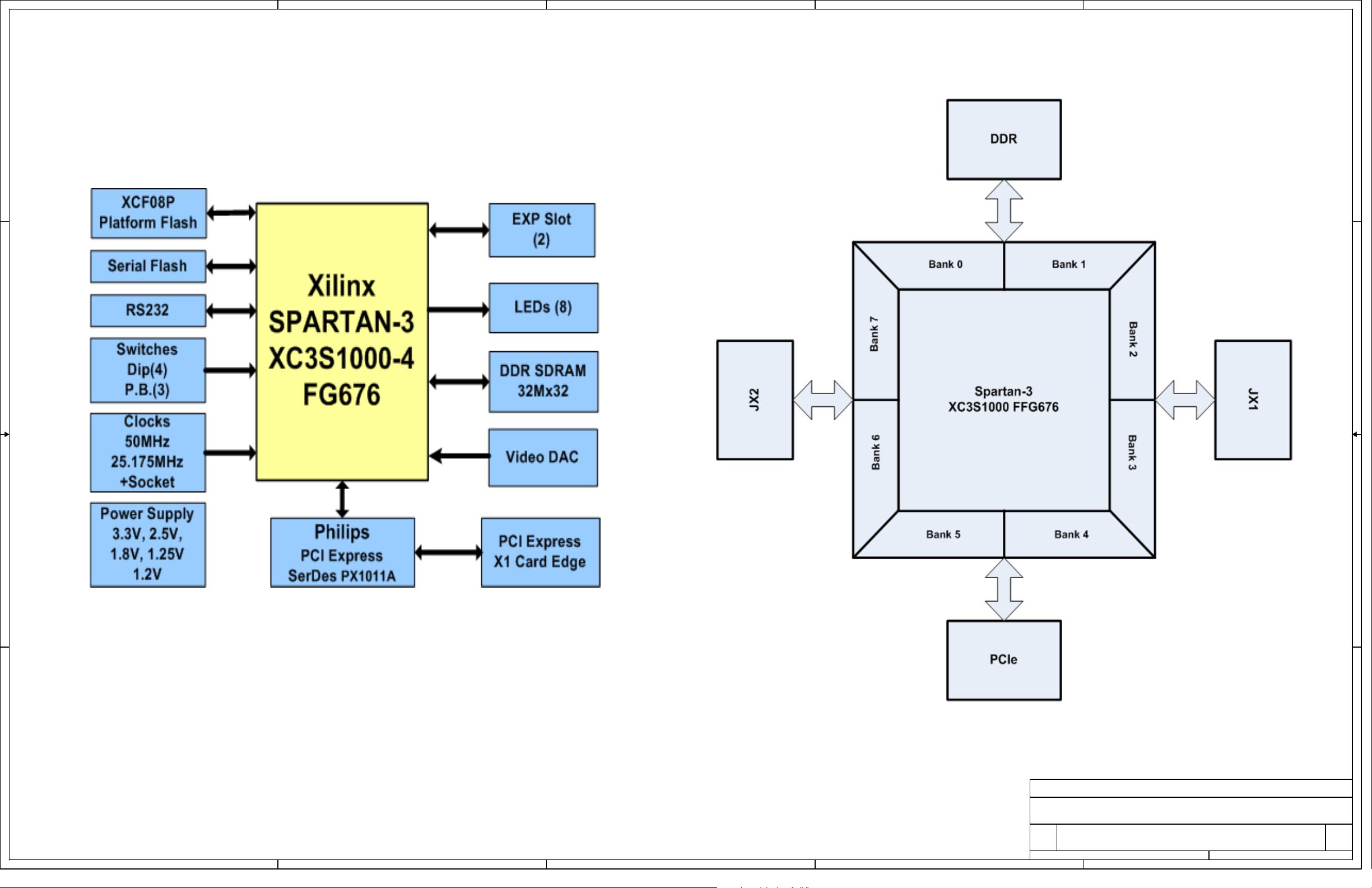
FPGA Power
Function
12
www.em.avnet.com/xilinx
1
Cover Sheet
6
4
FPGA - PCIe Banks 6 & 7
10
8
Board Power
Sheet Number
5
3FPGA - Banks 0 & 1
Avnet Engineering Services
11
7
9
FPGA Configuration
Copyright 2006, Avnet, Inc. All Rights Reserved.
This material may not be reproduced, distributed, republished, displayed, posted, transmitted or copied in
any form or by any means without the prior written permission of Avnet, Inc. AVNET and the AV logo are
registered trademarks of Avnet, Inc. All trademarks and trade names are the properties of their respective
owners and Avnet, Inc. disclaims any proprietary interest or right in trademarks, service marks and trade
names other than its own.
Avnet is not responsible for typographical or other errors or omissions or for direct, indirect, incidental or
consequential damages related to this material or resulting from its use. Avnet makes no warranty or
representation respecting this material, which is provided on an "AS IS" basis. AVNET HEREBY
DISCLAIMS ALL WARRANTIES OR LIABILITY OF ANY KIND WITH RESPECT THERETO, INCLUDING,
WITHOUT LIMITATION, REPRESENTATIONS REGARDING ACCURACY AND COMPLETENESS, ALL
IMPLIED WARRANTIES AND CONDITIONS OF MERCHANTABILITY, SUITABILITY OR FITNESS FOR A
PARTICULAR PURPOSE, TITLE AND/OR NON-INFRINGEMENT. This material is not designed, intended
or authorized for use in medical, life support, life sustaining or nuclear applications or applications in which
the failure of the product could result in personal injury, death or property damage. Any party using or
selling products for use in any such applications do so at their sole risk and agree that Avnet is not liable,
in whole or in part, for any claim or damage arising from such use, and agree to fully indemnify, defend and
hold harmless Avnet from and against any and all claims, damages, loss, cost, expense or liability arising
out of or in connection with the use or performance of products in such applications.
Spartan-3 PCIe Starter Board
REVISION 2.1
FPGA - Banks 2 & 3
FPGA - LVDS Banks 4 & 5
PCI Express
DDR SDRAM
Video DAC
2Block Diagram
13
Revision Notes
Powered By:

剩余12页未读,继续阅读
资源评论


