没有合适的资源?快使用搜索试试~ 我知道了~
可调 ldo芯片资料
需积分: 31 8 下载量 83 浏览量
2011-02-08
15:52:09
上传
评论
收藏 371KB PDF 举报
温馨提示
试读
16页
可调ldo LP38500-ADJ LP38500-ADJ LP38500-ADJ
资源推荐
资源详情
资源评论
LP38500/2-ADJ, LP38500A/
2A-ADJ
October 30, 2009
1.5A FlexCap Low Dropout Linear Regulator for 2.7V to
5.5V Inputs
General Description
National's FlexCap LDO's feature unique compensation that
allows the use of any type of output capacitor with no limits
on minimum or maximum ESR. The LP38500/2 series of low-
dropout linear regulators operates from a +2.7V to +5.5V input
supply. These ultra low dropout linear regulators respond very
quickly to step changes in load, which makes them suitable
for low voltage microprocessor applications. Developed on a
CMOS process, (utilizing a PMOS pass transistor), the
LP38500/2 has low quiescent current that changes little with
load current.
Ground Pin Current: Typically 2 mA at 1.5A load current.
Disable Mode: Typically 25 nA quiescent current when the
Enable pin is pulled low.
Simplified Compensation: Stable with any type of output
capacitor, regardless of ESR.
Precision Output: "A" grade versions available with 1.5%
V
ADJ
tolerance (25°C) and 3% over line, load and tempera-
ture.
Features
■
FlexCap: Stable with ceramic, tantalum, or aluminum
capacitors
■
Stable with 10 µF input/output capacitor
■
Adjustable output voltage from 0.6V to 5V
■
Low ground pin current
■
25 nA quiescent current in shutdown mode
■
Guaranteed output current of 1.5A
■
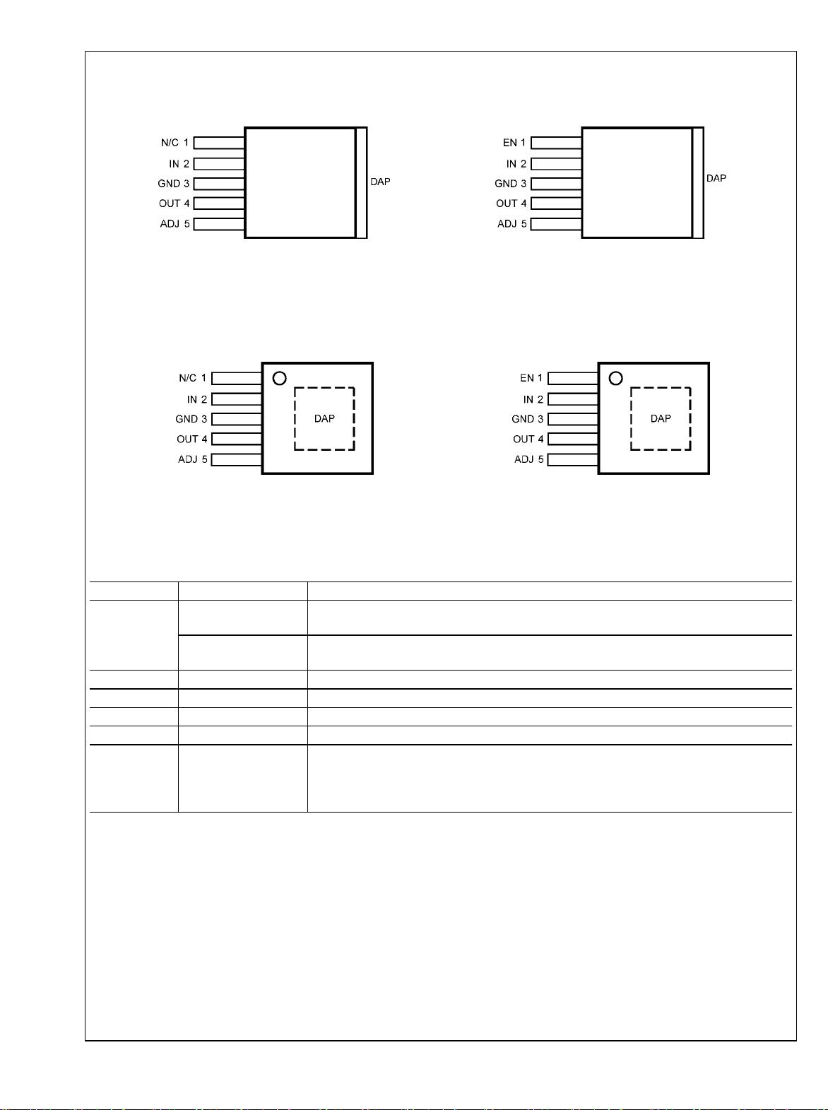
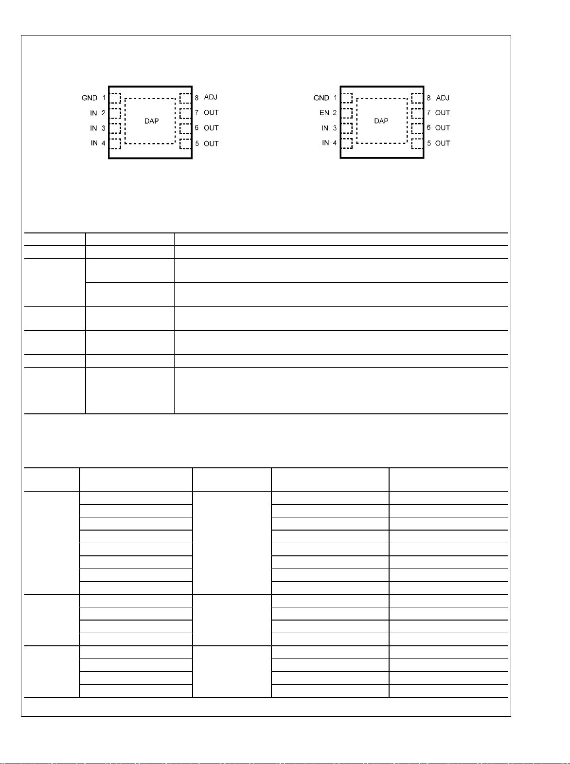
Available in TO-263, TO-263 THIN, and LLP-8 packages
■
Guaranteed V
ADJ
accuracy of ±1.5% @ 25°C (A Grade)
■
Guaranteed accuracy of ±3.5% @ 25°C (STD)
■
Over-Temperature and Over-Current protection
■
−40°C to +125°C operating T
J
range
■
Enable pin (LP38502)
Applications
■
ASIC Power Supplies In:
Printers, Graphics Cards, DVD Players
Set Top Boxes, Copiers, Routers
■
DSP and FPGA Power Supplies
■
SMPS Regulator
■
Conversion from 3.3V or 5V Rail
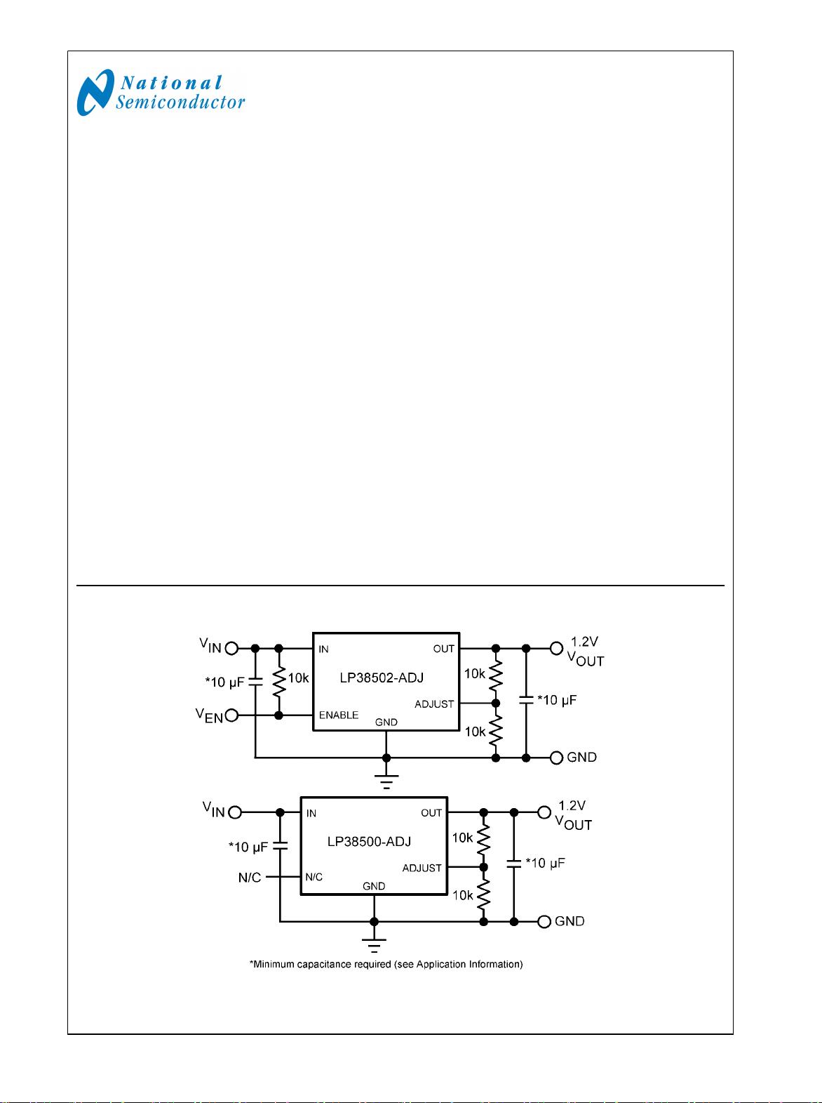
Typical Application Circuit
30036119
© 2009 National Semiconductor Corporation 300361 www.national.com
LP38500/2-ADJ, LP38500A/2A-ADJ 1.5A FlexCap Low Dropout Linear Regulator for 2.7V to 5.5V
Inputs
Connection Diagrams for TO-263 (TS) Package
30036121
Top View (LP38500TS-ADJ)
TO-263 Package
30036122
Top View (LP38502TS-ADJ)
TO-263 Package
Connection Diagrams for TO-263 THIN (TJ) Package
30036163
Top View (LP38500TJ-ADJ, LP38500ATJ-ADJ)
TO-263 THIN Package
30036162
Top View (LP38502TJ-ADJ, LP38502ATJ-ADJ)
TO-263 THIN Package
Pin Descriptions for TO-263 (TS), TO-263 THIN (TJ) Packages
Pin # Designation Function
1
EN
Enable (LP38502 only). Pull high to enable the output, low to disable the output. This pin has
no internal bias and must be either tied to the input voltage, or actively driven.
N/C
In the LP38500, this pin has no internal connections. It can be left floating or used for trace
routing.
2 IN Input Supply
3 GND Ground
4 OUT Regulated Output Voltage
5 ADJ Sets output voltage
DAP DAP
The DAP is used to remove heat from the device by conducting it to the copper clad area on
the PCB which acts as the heatsink. The DAP is electrically connected to the backside of the
die. The DAP must be connected to ground potential, but can not be used as the only ground
connection.
www.national.com 2
LP38500/2-ADJ, LP38500A/2A-ADJ
Connection Diagrams for LLP-8 (SD) Package
30036159
Top View (LP38500SD-ADJ, LP38500ASD-ADJ)
LLP-8 Package
30036160
Top View (LP38502SD-ADJ, LP38502ASD-ADJ)
LLP-8 Package
Pin Descriptions for LLP-8 (SD) Package
Pin # Designation Function
1 GND Ground
2
IN
Input Supply (LP38500 only). Input Supply pins share current and must be connected
together on the PC Board.
EN
Enable (LP38502 only). Pull high to enable the output, low to disable the output. This pin has
no internal bias and must be either tied to the input voltage, or actively driven.
3, 4 IN
Input Supply. Input Supply pins share current and must be connected together on the PC
Board.
5, 6, 7 OUT
Regulated Output Voltage. Output pins share current and must be connected together on the
PC Board.
8 ADJ Sets output voltage
DAP DAP
The DAP is used to remove heat from the device by conducting it to a copper clad area on
the PCB which acts as a heatsink. The DAP is electrically connected to the backside of the
die. The DAP must be connected to ground potential, but can not be used as the only ground
connection.
Ordering Information
TABLE 1. Package Marking and Ordering Information
Output
Voltage
Order Number
Package Type Package Marking Supplied As:
ADJ
LP38500SDX-ADJ
LLP-8
LP38500SD-ADJ Tape and Reel of 4500 Units
LP38500SD-ADJ LP38500SD-ADJ Tape and Reel of 1000 Units
LP38502SDX-ADJ LP38502SD-ADJ Tape and Reel of 4500 Units
LP38502SD-ADJ LP38502SD-ADJ Tape and Reel of 1000 Units
LP38500ASDX-ADJ LP38500ASD-ADJ Tape and Reel of 4500 Units
LP38500ASD-ADJ LP38500ASD-ADJ Tape and Reel of 1000 Units
LP38502ASDX-ADJ LP38502ASD-ADJ Tape and Reel of 4500 Units
LP38502ASD-ADJ LP38502ASD-ADJ Tape and Reel of 1000 Units
ADJ
LP38500TSX-ADJ
TO-263
LP38500TS-ADJ Tape and Reel of 500 Units
LP38500TS-ADJ LP38500TS-ADJ Rail of 45 Units
LP38502TSX-ADJ LP38502TS-ADJ Tape and Reel of 500 Units
LP38502TS-ADJ LP38502TS-ADJ Rail of 45 Units
ADJ
LP38500TJ-ADJ
TO-263 THIN
LP38500TJ-ADJ Tape and Reel of 1000 Units
LP38502TJ-ADJ LP38502TJ-ADJ Tape and Reel of 1000 Units
LP38500ATJ-ADJ LP38500ATJ-ADJ Tape and Reel of 1000 Units
LP38502ATJ-ADJ LP38502ATJ-ADJ Tape and Reel of 1000 Units
3 www.national.com
LP38500/2-ADJ, LP38500A/2A-ADJ
Absolute Maximum Ratings (Note 1)
If Military/Aerospace specified devices are required,
please contact the National Semiconductor Sales Office/
Distributors for availability and specifications.
Storage Temperature Range −65°C to +150°C
Lead Temperature
(Soldering, 5 sec.) 260°C
ESD Rating (Note 2) ±2 kV
Power Dissipation(Note 3) Internally Limited
Input Pin Voltage (Survival) −0.3V to +6.0V
Enable Pin Voltage (Survival) −0.3V to +6.0V
Output Pin Voltage (Survival) −0.3V to +6.0V
I
OUT
(Survival)
Internally Limited
Operating Ratings (Note 1)
Input Supply Voltage 2.7V to 5.5V
Enable Input Voltage 0.0V to 5.5V
Output Current (DC) 0 to 1.5A
Junction Temperature(Note 3) −40°C to +125°C
V
OUT
0.6V to 5V
Electrical Characteristics
LP38500/2–ADJ
Unless otherwise specified: V
IN
= 3.3V, I
OUT
= 10 mA, C
IN
= 10 µF, C
OUT
= 10 µF, V
EN
= V
IN
, V
OUT
= 1.8V. Limits in standard type
are for T
J
= 25°C only; limits in boldface type apply over the junction temperature (T
J
) range of -40°C to +125°C. Minimum and
Maximum limits are guaranteed through test, design, or statistical correlation. Typical values represent the most likely parametric
norm at T
J
= 25°C, and are provided for reference purposes only.
Symbol Parameter Conditions Min Typ Max Units
V
ADJ
Adjust Pin Voltage (Note 6)
2.7V ≤ V
IN
≤ 5.5V
10 mA ≤ I
OUT
≤ 1.5A
0.584
0.575
0.605
0.626
0.635
V
V
ADJ
Adjust Pin Voltage (Note 6)
"A" GRADE
2.7V ≤ V
IN
≤ 5.5V
10 mA ≤ I
OUT
≤ 1.5A
0.596
0.587
0.605
0.614
0.623
V
I
ADJ
Adjust Pin Bias Current
2.7V ≤ V
IN
≤ 5.5V
50 750 nA
V
DO
Dropout Voltage (Note 7)
I
OUT
= 1.5A
220
275
375
mV
ΔV
OUT
/ΔV
IN
Output Voltage Line
Regulation
(Note 4, Note 6)
2.7V ≤ V
IN
≤ 5.5V
—
0.04
0.05
—
%/V
ΔV
OUT
/ΔI
OUT
Output Voltage Load
Regulation
(Note 5, Note 6)
10 mA ≤ I
OUT
≤ 1.5A
—
0.18
0.33
—
%/A
I
GND
Ground Pin Current In Normal
Operation Mode
10 mA ≤ I
OUT
≤ 1.5A
—
2
3.5
4.5
mA
I
DISABLED
Ground Pin Current
V
EN
< V
IL(EN)
—
0.025
0.125
15
µA
I
OUT(PK)
Peak Output Current
V
OUT
≥ V
OUT(NOM)
- 5%
3.6 A
I
SC
Short Circuit Current
V
OUT
= 0V
2 3.7 A
Enable Input (LP38502 Only)
V
IH(EN)
Enable Logic High
V
OUT
= ON
1.4
— —
V
V
IL(EN)
Enable Logic Low
V
OUT
= OFF
— —
0.65
t
d(off)
Turn-off delay
Time from V
EN
< V
IL(EN)
to V
OUT
=
OFF
I
LOAD
= 1.5A
—
25
—
µs
t
d(on)
Turn-on delay
Time from V
EN
>V
IH(EN)
to V
OUT
=
ON
I
LOAD
= 1.5A
—
25
—
I
IH(EN)
Enable Pin High Current
V
EN
= V
IN
—
1
—
nA
I
IL(EN)
Enable Pin Low Current
V
EN
= 0V
—
0.1
—
www.national.com 4
LP38500/2-ADJ, LP38500A/2A-ADJ
剩余15页未读,继续阅读
资源评论
fw8888
- 粉丝: 0
- 资源: 13
上传资源 快速赚钱
- 我的内容管理 展开
- 我的资源 快来上传第一个资源
- 我的收益 登录查看自己的收益
- 我的积分 登录查看自己的积分
- 我的C币 登录后查看C币余额
- 我的收藏
- 我的下载
- 下载帮助
安全验证
文档复制为VIP权益,开通VIP直接复制
信息提交成功