
System Development User Guide
UG-992
One Technology Way • P. O. Box 9106 • Norwood, MA 02062-9106, U.S.A. • Tel: 781.329.4700 • Fax: 781.461.3113 • www.analog.com
System Development User Guide for the AD9371 Integrated,
Dual RF Transceiver with Observation Path
PLEASE SEE THE LAST PAGE FOR AN IMPORTANT
WARNING AND LEGAL TERMS AND CONDITIONS.
Rev. A | Page 1 of 307
INTRODUCTION
This user guide is the main source of information for systems
engineers and software developers using the AD9371 software
defined radio transceiver. The sections in this user guide are
organized to make it easier for users to find the information
pertinent to their area of interest. These sections are as folllows:
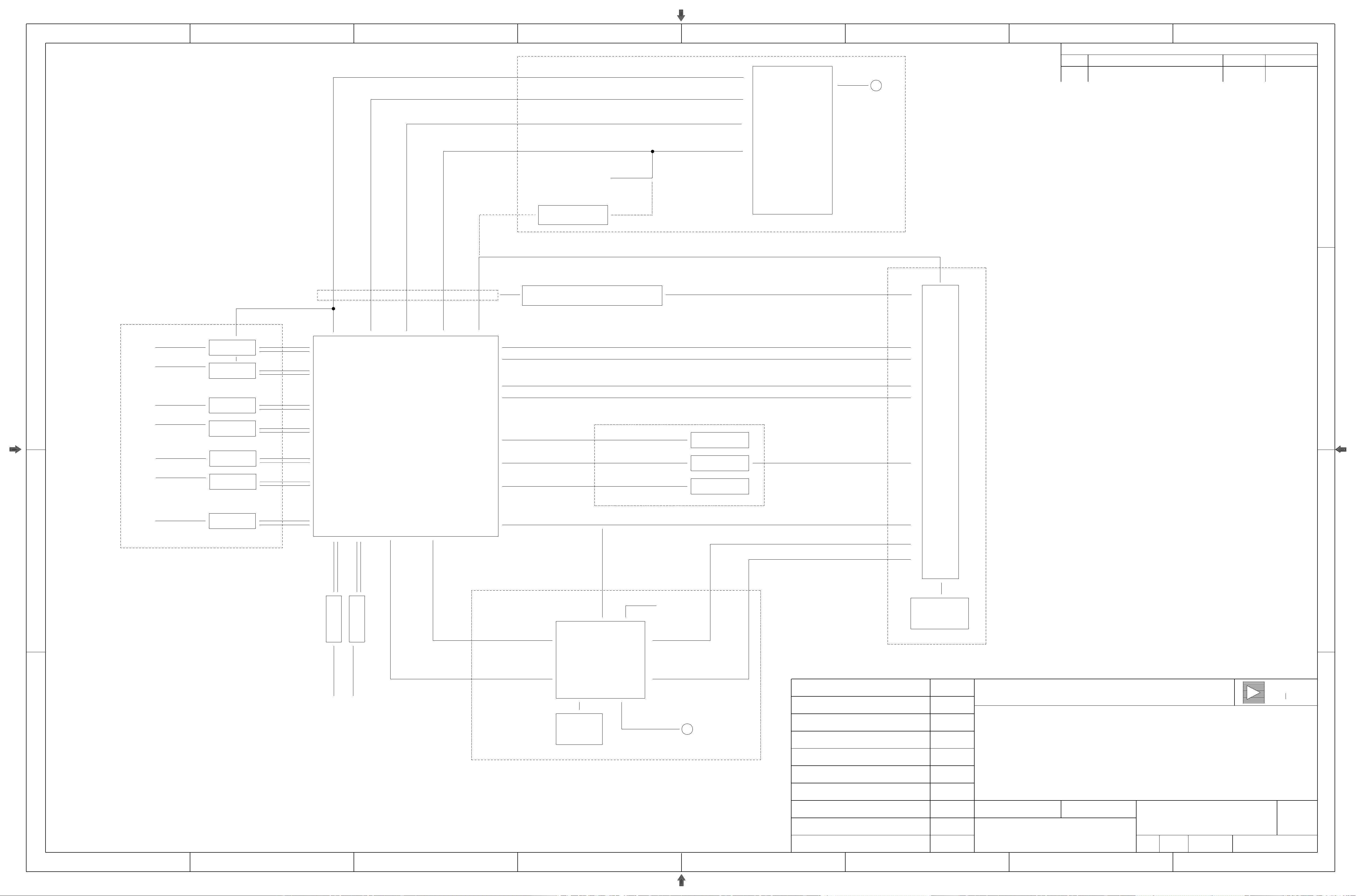
• System Overview. This section explains the capability of
the device and serves as an introduction to all the subsystems
and functions, including the block diagrams and interfaces.
• System Architecture Description. This section explains the
software design approach using the application
programming interface (API) and all details required to
develop code on the device.
• Software Integration. This section describes the process for
developing code using the AD9371 APIs. This section lists
common API functions for user integration into the code
base.
• Serial Peripheral Interface (SPI). The SPI is the main
control interface between the baseband processor (BBP)
and the integrated transceiver.
• JESD204B Interface. This section provides a description of
the JESD204B digital interface, setup, and configuration
options.
• System Initialization. This section provides the sequence of
steps required at startup.
• Quadrature Error Correction, Calibration, and ARM
Configuration. This section describes the calibration and
error correction functions and setup guidelines for
configuring the ARM processor to perform scheduled
adjustments.
• System Control. This section describes the commands and
sequences for setting up the different radio channels.
• Tx Power Control. This section explains the commands
and procedures for adjusting Tx power control during
normal operation.
• Reference Clock and SYSREF Connections. This section
describes how to set up the reference clocks needed for all
internal clock and signal generation as well as data
synchronization.
• Synthesizer Configuration. This section describes how to
configure the synthesizers for different modes of operation.
This section includes details for receiver (Rx), transmitter
(Tx), observation receiver (ORx), and clock phase-locked
loop (PLL) setup, as well as the calibration PLL setup.
• Gain Control. This section describes the options for
controlling receiver gain settings, including manual gain
control (MGC) provided by the BBP and automatic gain
control (AGC) provided by the integrated transceiver.
• Filter Configuration. This section describes all the digital
filter blocks in the the receivers and transmitters, and explains
the programmable FIR filters and how to set their coefficients.
• Observation Receiver. This section describes the ORx inputs
and the sniffer receiver (SnRx) inputs, including system
implementation and setup APIs.
• TDD Configuration and Setup. This section describes
software configuration to operate in a time division
duplexed (TDD) system.
• General-Purpose Input/Output (GPIO) Configuration.
This section describes the options for configuring standard
digital GPIO pins.
• 3.3 V General-Purpose Input/Output Overview. This
section describes the options for configuring the 3.3 V
supplied GPIO pins.
• General-Purpose Interrupt Overview. This section describes
setup and operation of the general-purpose interrupt pin.
• Auxilliary Converters—AUXDAC_x, AUXADC. This
section describes the capability of the AUXADC_x inputs,
the AUXDAC_x outputs, and how to properly configure
the inputs and outputs for various applications.
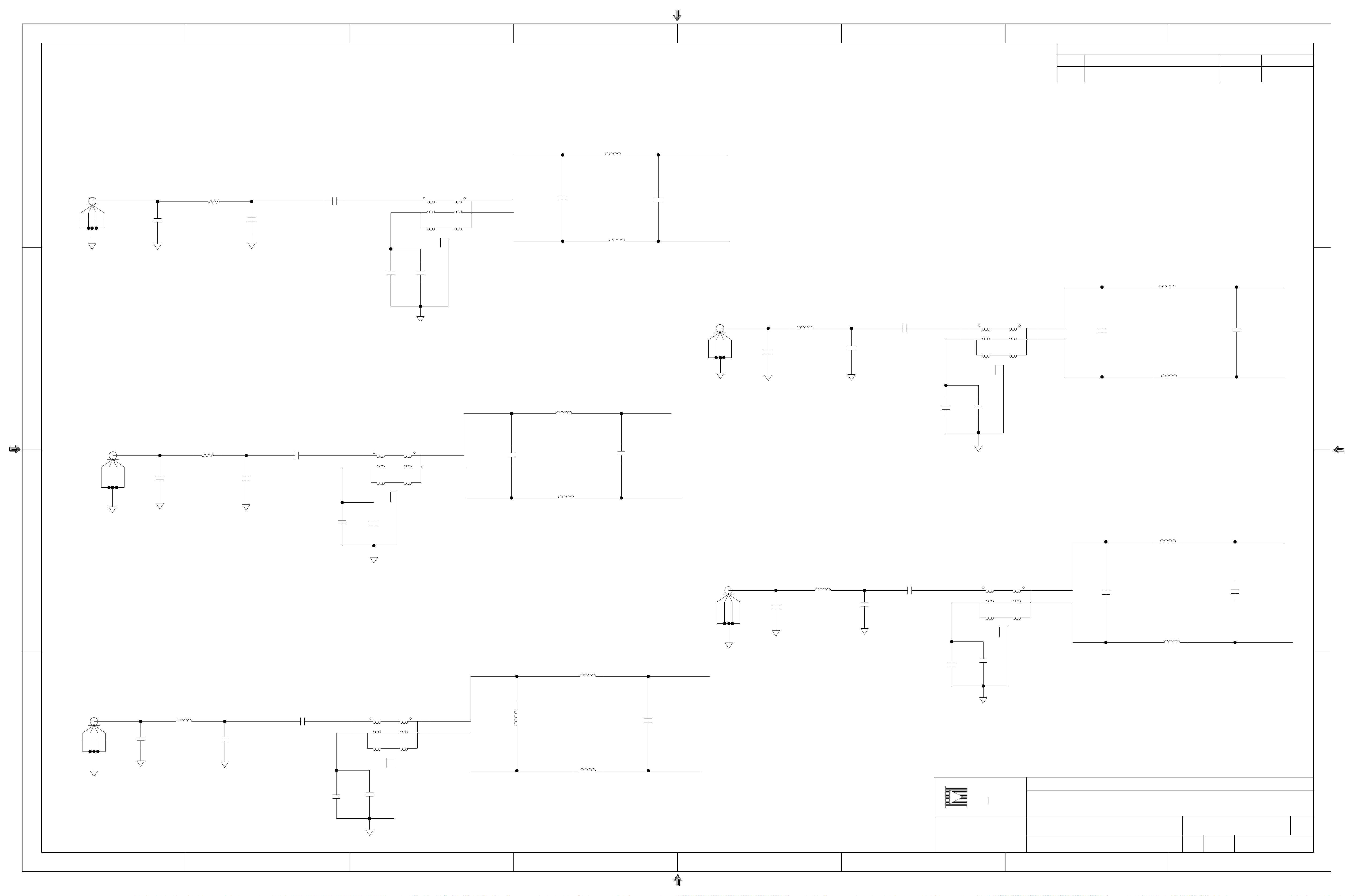
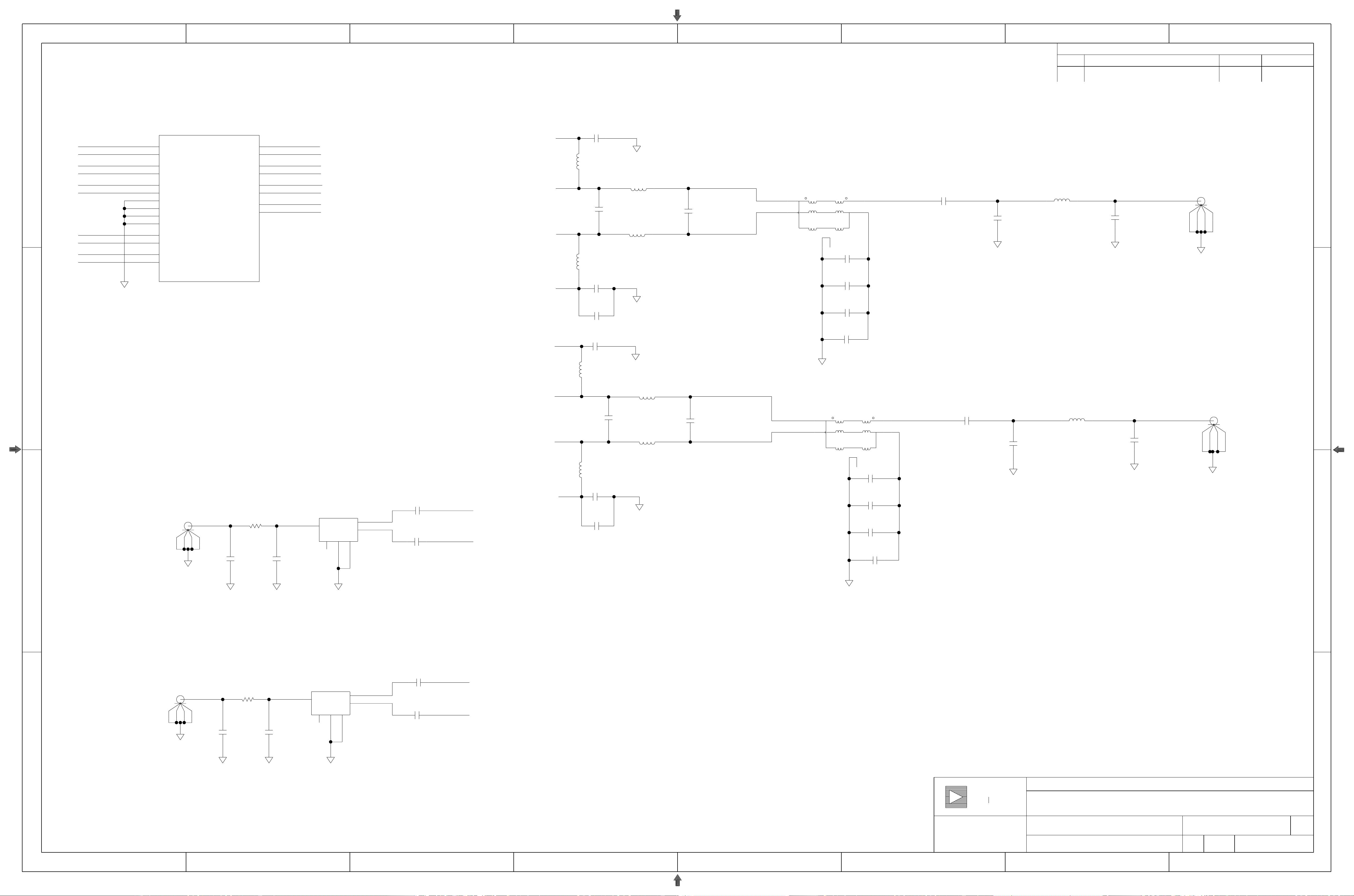
• RF Port Interface. This section explains all the details
necessary to properly match the RF impedances of each
differential input and output port.
• Printed Circuit Board Layout Guidelines. This section
describes the printed circuit board (PCB) construction,
layout, routing, and isolation techniques necessary to
optimize
AD9371 performance.
• Power Management Considerations. This section describes
the power supply design and all the considerations needed
to optimize AD9371 performance.
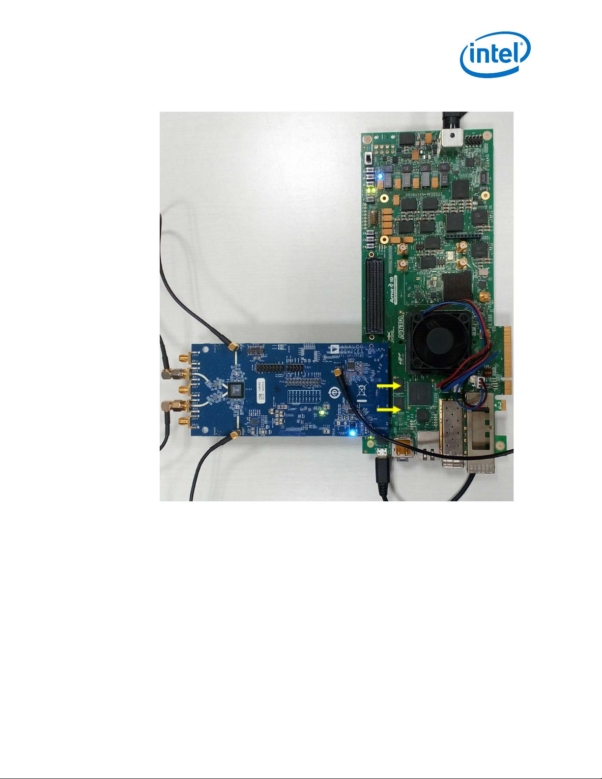
• AD9371 Demonstration System Overview. This section
describes the AD9371 demonstration system, including the
evaluation board, motherboard, and hardware integration
setup needed to properly evaluate device performance.
• AD9371 Transceiver Evaluation Software (TES). This
section describes the AD9371 transceiver evaluation
software (TES) that provides a graphical user interface that
controls the evaluation system.