没有合适的资源?快使用搜索试试~ 我知道了~
RFFC2072 datasheet
5星 · 超过95%的资源 需积分: 10 67 下载量 76 浏览量
2011-06-10
10:13:49
上传
评论 3
收藏 2.03MB PDF 举报
温馨提示
试读
23页
RFFC2072 datasheet 需要编程手册可以点击PDF中的链接
资源推荐
资源详情
资源评论
1 of 23
Optimum Technology Matching® Applied
GaAs HBT
InGaP HBT
GaAs MESFET
SiGe BiCMOS
Si BiCMOS
SiGe HBT
GaAs pHEMT
Si CMOS
Si BJT
GaN HEMT
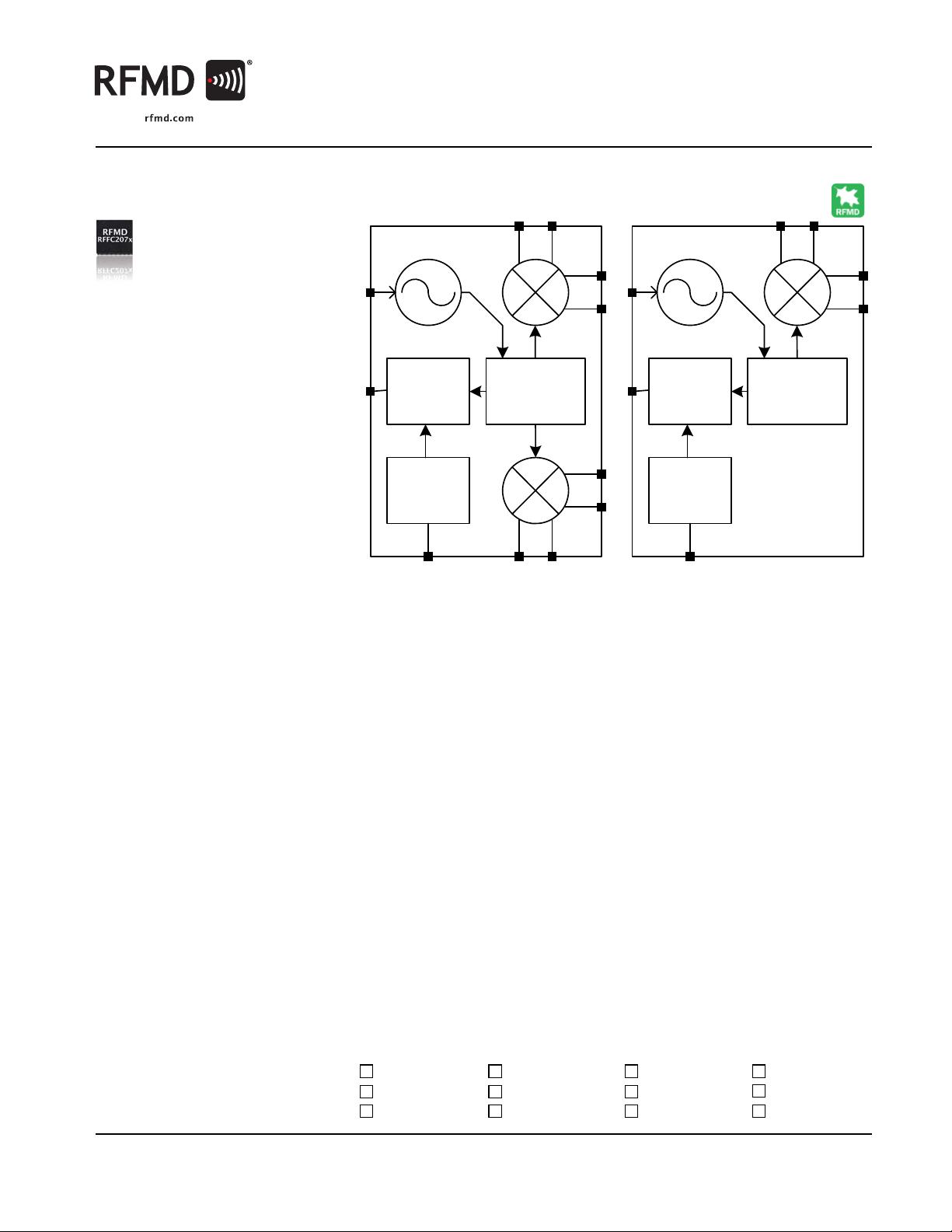
Functional Block Diagram
RF MICRO DEVICES®, RFMD®, Optimum Technology Matching®, Enabling Wireless Connectivity™, PowerStar®, POLARIS™ TOTAL RADIO™ and UltimateBlue™ are trademarks of RFMD, LLC. BLUETOOTH is a trade-
mark owned by Bluetooth SIG, Inc., U.S.A. and licensed for use by RFMD. All other trade names, trademarks and registered trademarks are the property of their respective owners. ©2006, RF Micro Devices, Inc.
Product Description
7628 Thorndike Road, Greensboro, NC 27409-9421 · For sales or technical
support, contact RFMD at (+1) 336-678-5570 or sales-support@rfmd.com.
BiFET HBT
LDMOS
Synth
Phase
det.
Ref.
divider
RFFC2071
Synth
Phase
det.
Ref.
divider
RFFC2072
RFFC2071/2072
2.7GHz RF SYNTHESIZER/VCO WITH
INTEGRATED RF MIXER
The RFFC2071 and RFFC2072 are re-configurable frequency conversion devices
with integrated fractional-N phased locked loop (PLL) synthesizer, voltage con-
trolled oscillator (VCO) and either one or two high linearity mixers. The fractional-N
synthesizer takes advantage of an advanced sigma-delta modulator that delivers
ultra-fine step sizes and low spurious products. The PLL/VCO engine combined with
an external loop filter allows the user to generate local oscillator (LO) signals from
85MHz to 2700MHz. The LO signal is buffered and routed to the integrated RF mix-
ers which are used to up/down-convert frequencies ranging from 30MHz to
2700MHz. The mixer bias current is programmable and can be reduced for applica-
tions requiring lower power consumption. Both devices can be configured to work
as signal sources by bypassing the integrated mixers. Device programming is
achieved via a simple 3-wire serial interface. In addition, a unique programming
mode allows up to four devices to be controlled from a common serial bus. This
eliminates the need for separate chip-select control lines between each device and
the host controller. Up to six general purpose outputs are provided, which can be
used to access internal signals (e.g. the LOCK signal) or to control front end compo-
nents. Both devices operate with a 2.7V to 3.3V power supply.
Features
85MHz to 2700MHz LO
Frequency Range
Fractional-N Synthesizer with
Very Low Spurious Levels
Typical Step Size 1.5Hz
Fully Integrated Low Phase Noise
VCO and LO Buffers
Integrated Phase Noise
0.18°rms
at 1GHz
High Linearity RF Mixer(s)
30MHz to 2700MHz Mixer
Frequency Range
Input IP3 +23dBm
Mixer Bias Adjustable for Low
Power Operation
Full Duplex Mode (RFFC2071)
2.7V to 3.3V Power Supply
Low Current Consumption
3- or 4-Wire Serial Interface
Applications
CATV Head-Ends
Digital TV Repeaters
Multi-Dwelling Units
Diversity Receivers
Software Defined Radios
Frequency Band Shifters
Point-to-Point Radios
Cellular Repeaters
WiMax/LTE Infrastructure
Cellular Jammers
Satellite Communications
VHF/UHF Radios
DS100920
Package: QFN, 32-Pin, 5mmx5mm
RFFC2071/20
72 2.7 GHz
RF Synthe-
sizer/VCO with
Integrated RF
Mixer
2 of 23
RFFC2071/2072
DS100920
7628 Thorndike Road, Greensboro, NC 27409-9421 · For sales or technical
support, contact RFMD at (+1) 336-678-5570 or sales-support@rfmd.com.
Absolute Maximum Ratings
Parameter Rating Unit
Supply Voltage (V
DD
) -0.5 to +3.6 V
Input Voltage (V
IN
) any pin -0.3 to V
DD
+0.3 V
RF/IF mixer input power +15 dBm
Operating Temperature Range -40 to +85 °C
Storage Temperature Range -40 to +150 °C
Parameter
Specification
Unit Condition
Min. Typ. Max.
ESD Requirementsl
Human Body Model 2000 V General
1000 V RF Pins
Machine Model 200 V General
100 V RF Pins
Operating Conditions
Supply voltage (V
DD
) 2.7 3.0 3.3 V
Temperature (T
OP
)-40 +85°C
Logic Inputs/Outputs (V
DD
=Supply to DIG_VDD pin)
Input low voltage -0.3 +0.5 V
Input high voltage 1.5 V
DD
V
Input low current -10 +10 uA Input=0V
Input high current -10 +10 uA Input=V
DD
Output low voltage 0 0.2*V
DD
V
Output high voltage 0.8*V
DD
V
DD
V
Load resistance 10 k
Load capacitance 20 pF
GPO Drive Capability
Sink Current 20 mA at V
OL
=0.6V
Source Current 20 mA at V
OL
=2.4V
Output Impedance 25 Ω
Static
Supply Current (I
DD
) with 1GHz LO 100 mA Low current, MIX_IDD=1, one mixer enabled.
125 mA High linearity, MIX_IDD=6, one mixer enabled.
Standby 2 mA Reference oscillator and bandgap only.
Power Down Current 300 uA ENBL=0 and REF_STBY=0
Mixer 1/2 (Mixer output driving 4:1 balun)
Gain -2 dB Not including balun losses
Noise Figure 10 dB Low current setting
13 dB High linearity setting
IIP3 +10 dBm Low current setting
+23 dBm High linearity setting
Input port frequency range 30 2700 MHz
Mixer input return loss 10 dB 100 differential
Output port frequency range 30 2700 MHz
Caution! ESD sensitive device.
Exceeding any one or a combination of the Absolute Maximum Rating conditions may
cause permanent damage to the device. Extended application of Absolute Maximum
Rating conditions to the device may reduce device reliability. Specified typical perfor-
mance or functional operation of the device under Absolute Maximum Rating condi-
tions is not implied.
RoHS status based on EUDirective2002/95/EC (at time of this document revision).
The information in this publication is believed to be accurate and reliable. However, no
responsibility is assumed by RF Micro Devices, Inc. ("RFMD") for its use, nor for any
infringement of patents, or other rights of third parties, resulting from its use. No
license is granted by implication or otherwise under any patent or patent rights of
RFMD. RFMD reserves the right to change component circuitry, recommended appli-
cation circuitry and specifications at any time without prior notice.
3 of 23
RFFC2071/2072
DS100920
7628 Thorndike Road, Greensboro, NC 27409-9421 · For sales or technical
support, contact RFMD at (+1) 336-678-5570 or sales-support@rfmd.com.
Parameter
Specification
Unit Condition
Min. Typ. Max.
Reference Oscillator
External reference frequency 10 104 MHz
Reference divider ratio 1 7
External reference input level 500 800 1500 mVp-p AC-coupled
Synthesizer (Loop bandwidth of 200KHz, 52MHz reference)
Synthesizer output frequency 85 2700 MHz
Phase detector frequency 52 MHz
Phase noise (LO=1GHz) -108 dBc/Hz 10kHz offset
-108 dBc/Hz 100kHz offset
-135 dBc/Hz 1MHz offset
0.19 ° RMS integrated from 1kHz to 40MHz
Phase noise (LO=2GHz) -102 dBc/Hz 10kHz offset
-102 dBc/Hz 100kHz offset
-130 dBc/Hz 1MHz offset
0.32 ° RMS integrated from 1kHz to 40MHz
Normalized phase noise floor -214 dBc/Hz Measured at 20kHz to 30kHz offset
Voltage Controlled Oscillator
Open loop phase noise at 1MHz
offset
2.5GHz LO frequency -134 dBc/Hz VCO3
2.0GHz LO frequency -135 dBc/Hz VCO2
1.5GHz LO frequency -136 dBc/Hz VCO1
Open loop phase noise at 10MHz
offset
2.5GHz LO frequency -149 dBc/Hz VCO3
2.0GHz LO frequency -150 dBc/Hz VCO2
1.5GHz LO frequency -151 dBc/Hz VCO1
4 of 23
RFFC2071/2072
DS100920
7628 Thorndike Road, Greensboro, NC 27409-9421 · For sales or technical
support, contact RFMD at (+1) 336-678-5570 or sales-support@rfmd.com.
Note 1: An RC low pass filter could be used on this line to reduce digital noise.
Note 2: If the device is under software control this input can be configured as a general purpose output (GPO).
Note 3: Connect a 51k resistor from this pin to ground, this pin is sensitive to low frequency noise injection.
Note 4: DC voltage should not be applied to this pin. Use either an AC-coupling capacitor as part of lumped element matching
network or a transformer (see evaluation board schematic).
Note 5: This pin must be connected to ANA_VDD2 using an RF choke or a transformer (see application schematic).
Pin Function Description
1ENBL/GPO5
Device Enable pin. See note 1 and 2.
2EXT_LO
External local oscillator input.
3EXT_LO_DEC
Decoupling pin for external local oscillator.
4REXT
External bandgap bias resistor. See note 3.
5ANA_VDD1
Analog supply. Use good RF decoupling.
6LFILT1
Phase detector output. Low-frequency noise-sensitive node.
7LFILT2
Loop filter op-amp output. Low-frequency noise-sensitive node.
8LFILT3
VCO control input. Low-frequency noise-sensitive node.
9 MODE/GPO6
Mode select pin. See note 1 and 2.
10 REF_IN
Reference input. Use AC coupling capacitor.
11 NC
12 TM
Connect to ground.
13 MIX1_IPN
Differential input 1 (see note 4). On RFFC2072 this pin is NC.
14 MIX1_IPP
Differential input 1 (see note 4). On RFFC2072 this pin is NC.
15 GPO1/ADD1
General purpose output / MultiSlice address bit.
16 GPO2/ADD2
General purpose output / MultiSlice address bit.
17 MIX1_OPN
Differential output 1 (see note 5). On RFFC2072 this pin is NC.
18 MIX1_OPP
Differential output 1 (see note 5). On RFFC2072 this pin is NC.
19 DIG_VDD
Digital supply. Should be decoupled as close to the pin as possible.
20 NC
21 NC
22 ANA_VDD2
Analog supply. Use good RF decoupling.
23 MIX2_IPP
Differential input 2 (see note 4).
24 MIX2_IPN
Differential input 2 (see note 4).
25 GPO3/FM
General purpose output / frequency control input.
26 GPO4/LD/DO
General purpose output / Lock detect output / serial data out.
27 MIX2_OPN
Differential output 2 (see note 5).
28 MIX2_OPP
Differential output 2 (see note 5).
29 RESETX
Chip reset (active low). Connect to DIG_VDD if asynchronous reset is not required.
30 ENX
Serial interface select (active low). See note 1.
31 SCLK
Serial interface clock. See note 1.
32 SDATA
Serial interface data. See note 1.
Exposed paddle
Ground reference, should be connected to PCB ground through a low impedance path.
5 of 23
RFFC2071/2072
DS100920
7628 Thorndike Road, Greensboro, NC 27409-9421 · For sales or technical
support, contact RFMD at (+1) 336-678-5570 or sales-support@rfmd.com.
Theory of Operation
The RFFC2071 and RFFC2072 are wideband RF frequency converter chips which include a fractional-N synthesizer and a low
noise VCO core. The RFFC2071 has an LO signal multiplexer, two LO buffer circuits, and two RF mixers. The RFFC2072 has a
single LO buffer circuit and one RF mixer. Both devices have an integrated voltage reference and low drop out regulators sup-
plying critical circuit blocks such as the VCOs and synthesizer. Synthesizer programming, device configuration and control are
achieved through a mixture of hardware and software controls. All on-chip registers are programmed through a simple 3-wire
serial interface.
VCO
The VCO core in the RFFC2071 and RFFC2072 consists of three VCOs which, in conjunction with the integrated LO dividers of
/2 to /32, cover the LO range of 85MHz to 2700MHz. Each VCO has 128 overlapping bands which are used to achieve low
VCO gain and optimal phase noise performance across the whole tuning range. The chip automatically selects the correct VCO
(VCO auto-select) and VCO band (VCO coarse tuning) to generate the desired LO frequency based on the values programmed
into the PLL1 and PLL2 registers banks.
The VCO auto-select and VCO coarse tuning are triggered every time ENBL is taken high, or if the PLL re-lock self clearing bit is
programmed high. Once the correct VCO and band have been selected the PLL will lock onto the correct frequency. During the
band selection process, fixed capacitance elements are progressively connected to the VCO resonant circuit until the VCO is
oscillating approximately at the correct frequency. The output of this band selection, CT_CAL, is made available in the read-
back register. A value of 127 or 0 in this register indicates that the coarse tuning was unsuccessful, and this will also be indi-
cated by the CT_FAILED flag also available in the read-back register. A CT_CAL value between 1 and 126 indicates a success-
ful calibration, the actual value being dependent on the desired frequency as well as process variation for a particular device.
The band select process will center the VCO tuning voltage at about 1.0V, compensating for manufacturing tolerances and pro-
cess variation as well as environmental factors including temperature. In applications where the device is left enabled at the
same LO frequency for some time, it is recommended that automatic band selection be performed for every 30°C change in
temperature. This assumes an active loop filter.
The RFFC2071 and RFFC2072 feature a differential LO input to allow the mixer to be driven from an external LO source. The
fractional-N PLL can be used with an external VCO driven into this LO input, which may be useful to reduce phase noise in
some applications. This may also require an external op-amp, dependant on the tuning voltage required by the external VCO.
In the RFFC2071 the LO signal is routed to mixer 1, mixer 2, or both mixers depending on the state of the MODE pin (or MODE
bit if under software control) and the value of the FULLD bit. Setting FULLD high puts the device into Full Duplex mode and both
mixers are enabled.
Fractional-N PLL
The RFFC2071 and RFFC2072 contain a charge pump-based fractional-N phase locked loop (PLL) for controlling the three
VCOs. The PLL includes automatic calibration systems to counteract the effects of process and environmental variations,
ensuring repeatable loop response and phase noise performance. As well as the VCO auto-select and coarse tuning, there is a
loop filter calibration mechanism which can be enabled if required. This operates by adjusting the charge pump current to
maintain loop bandwidth. This can be useful for applications where the LO is tuned over a wide frequency range.
The PLL has been designed to use a reference frequency of between 10MHz and 104MHz from an external source, which is
typically a temperature controlled crystal oscillator (TCXO). A reference divider (divide by 1 to divide by 7) is supplied and
should be programmed to limit the frequency at the phase detector to a maximum of 52MHz.
Two PLL programming banks are provided, the first bank is preceded by the label PLL1 and the second bank is preceded by the
label PLL2. For the RFFC2071 these banks are used to program mixer 1 and mixer 2 respectively, and are selected automati-
cally as the mixer is selected using MODE. For the RFFC2072 mixer 2 and register bank PLL2 are normally used.
The VCO outputs are first divided down, typically by two, in a high frequency prescalar. The output of this high frequency pres-
calar then enters the N divider, which is a fractional divider containing a dual-modulus prescaler and a digitally spur-compen-
剩余22页未读,继续阅读
资源评论
- ~~懒懒2018-01-12挺好用的,最近的项目刚好用到这个芯片。谢谢分享。
- u0135607952014-06-27挺好用的 谢谢
- 飘飘小沙鸥2014-01-14终于找到了此芯片PDF呢~ 不错~ 非常感谢!
- 队长丶别开枪2016-09-10英文的略费劲啊 不过还是很有用的
- cx1235897162013-08-07挺好用的 谢谢
brownheart
- 粉丝: 0
- 资源: 3
上传资源 快速赚钱
- 我的内容管理 展开
- 我的资源 快来上传第一个资源
- 我的收益 登录查看自己的收益
- 我的积分 登录查看自己的积分
- 我的C币 登录后查看C币余额
- 我的收藏
- 我的下载
- 下载帮助
安全验证
文档复制为VIP权益,开通VIP直接复制
信息提交成功