没有合适的资源?快使用搜索试试~ 我知道了~
资源推荐
资源详情
资源评论
NIOS II Processor Booting Methods In MAX 10 Devices
2015.01.23
AN-730
Subscribe
Send Feedback
MAX
®
10 device is the first MAX device series which supports Nios
®
II processor.
Overview
MAX 10 devices contain on-chip flash which segmented to two types:
• Configuration Flash Memory (CFM) to store hardware configuration settings for MAX 10 FPGA
• User Flash Memory (UFM) to store user software applications
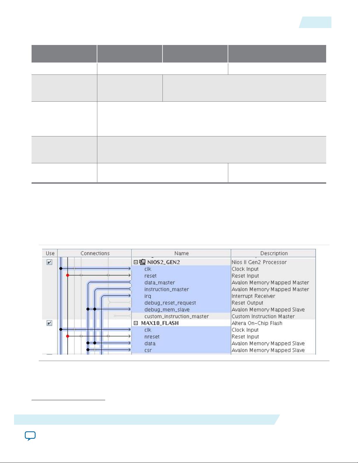
You can boot and configure the Nios II soft core processor to execute code from the on-chip flash within
the FPGA using the Altera On-chip Flash IP core.
This document describe the overview of the Altera On-chip Flash IP core and various booting
methodology using the MAX 10 on-chip flash.
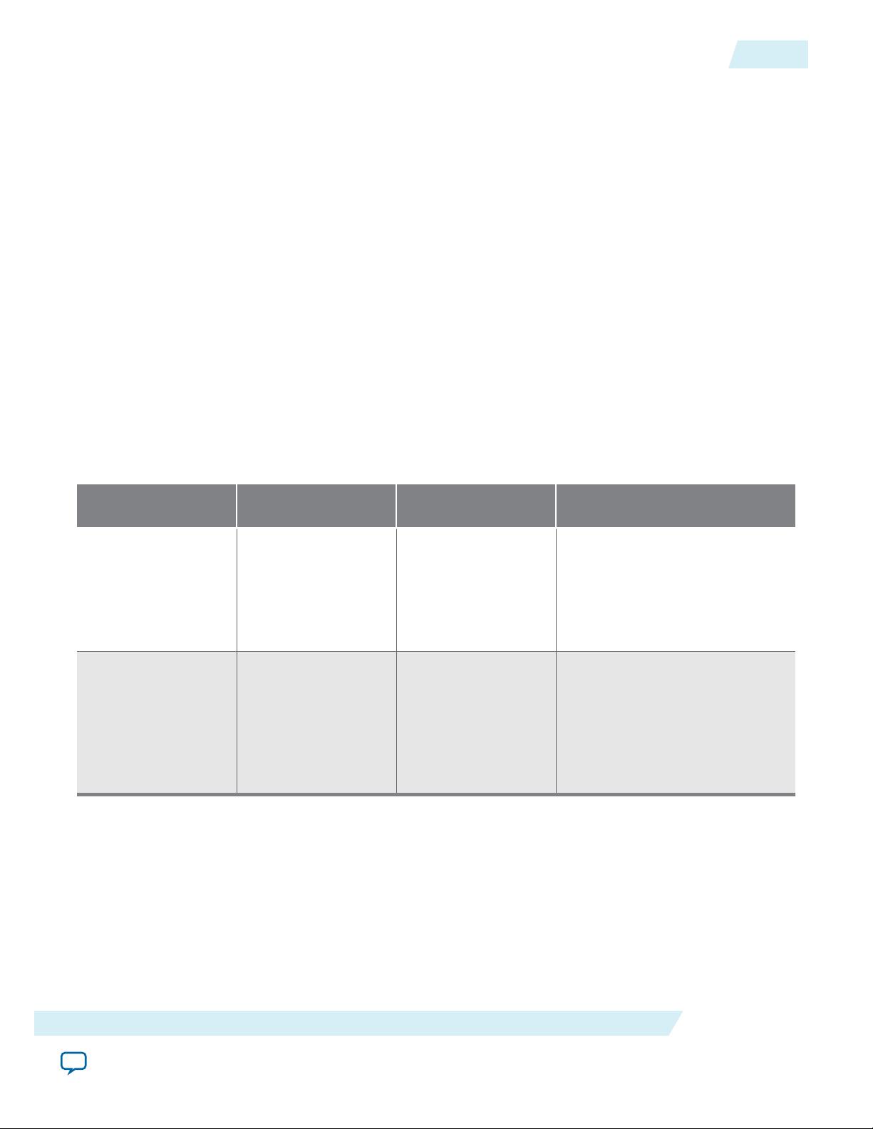
Abbreviations
Table 1: Abbreviations Use In the Document
Abbreviation Description
RAM Random Access Memory
OCRAM On-Chip RAM
UFM User Flash Memory
CFM Configuration Flash Memory
SBT Software Build Tools
HEX Hexadecimal File
This is an ASCII text file with the extension of .hex which
stores the initial memory values for a memory block.
XIP Execute In Place
POF Programmer Object File
ERAM Embedded Random Access Memory
©
2015 Altera Corporation. All rights reserved. ALTERA, ARRIA, CYCLONE, ENPIRION, MAX, MEGACORE, NIOS, QUARTUS and STRATIX words and logos are
trademarks of Altera Corporation and registered in the U.S. Patent and Trademark Office and in other countries. All other words and logos identified as
trademarks or service marks are the property of their respective holders as described at www.altera.com/common/legal.html. Altera warrants performance
of its semiconductor products to current specifications in accordance with Altera's standard warranty, but reserves the right to make changes to any
products and services at any time without notice. Altera assumes no responsibility or liability arising out of the application or use of any information,
product, or service described herein except as expressly agreed to in writing by Altera. Altera customers are advised to obtain the latest version of device
specifications before relying on any published information and before placing orders for products or services.
ISO
9001:2008
Registered
www.altera.com
101 Innovation Drive, San Jose, CA 95134
Prerequisite
You are required to have the knowledge of instantiating and developing a system with Nios II processor
based system. Altera recommends you to go through the online tutorials and training materials provided
at http://www.altera.com/education/edu-index.html before using this application note.
Related Information
• Nios II Gen2 Hardware Development Tutorial. A step by step procedure to build a Nios II Gen2
soft core processor system.
• Getting Started with the Graphical User Interface. This document provides the details of Nios II
Software Build Tools using graphical user interface.
MAX 10 On-chip Flash Overview
The MAX 10 On-chip Flash consists of two flash sectors with the functionality shown in the following
table.
Table 2: On-chip Flash Sectors in MAX 10 Devices
Flash Sector Functionality
Configuration Flash Memory (sectors
CFM0-2)
FPGA configuration file storage
User Flash Memory (sectors UFM0-1) User application or data storage
You can configure the CFM sector to use as UFM sector. The following table shows the storage location of
the configuration images based on internal configuration mode options available in MAX 10 devices. You
can refer to MAX 10 FPGA Configuration User Guide for more information related to the internal
configuration modes supported in MAX 10 devices.
2
Prerequisite
AN-730
2015.01.23
Altera Corporation
NIOS II Processor Booting Methods In MAX 10 Devices
Send Feedback
Table 3: Storage Location Of The Configuration Images Per Internal Configuration Mode Options
Internal Configuration
Modes
CFM2
(1)
CFM1
(1)
CFM0
Dual images Compressed Image 2 Compressed Image 1
Single
uncompressed
image
UFM Uncompressed image
Single
uncompressed
image with Memory
Initialization
Uncompressed image (with ERAM preload)
Single compressed
image with Memory
Initialization
Compressed image (with ERAM preload)
Single compressed
image
UFM Compressed Image
You must use the Altera On-chip Flash IP core to access to the flash memory in MAX 10 devices. You can
instantiate and connect the Altera On-chip Flash IP to the Nios II processor using the Qsys system in
Quartus II software. The Nios II soft core processor uses the Avalon
®
Memory-Mapped (Avalon-MM)
interface to communicate with the Altera On-chip Flash IP.
Figure 1: Example of Connections for The Altera On-chip Flash IP and the Nios II Gen2 Soft Core
Processor
Related Information
• MAX 10 FPGA Configuration User Guide
(1)
This sector is NOT supported in 10M02 device.
AN-730
2015.01.23
MAX 10 On-chip Flash Overview
3
NIOS II Processor Booting Methods In MAX 10 Devices
Altera Corporation
Send Feedback
• MAX 10 User Flash Memory User Guide
Altera On-chip Flash IP Architecture and Features
The Altera On-chip Flash IP core provides access to five flash sectors:
• UFM0
• UFM1
• CFM0
• CFM1
• CFM2
Important facts about UFM and CFM sectors:
• CFM sectors are intended for configuration (bitstream) data (*.pof) storage.
• You can store user data in the UFM sectors.
• Certain devices do not have a UFM1 sector. You can refer to UFM and CFM Array Size table for
available sectors per MAX 10 devices.
• You can configure CFM2 as a virtual UFM using “Single Uncompressed Image” internal configuration
mode.
• You can configure CFM2 and CFM1 as a virtual UFM using “Single Compressed Image” internal
configuration mode.
• The sizes of each sector varies with the selected MAX 10 devices.
Table 4: UFM and CFM Array Size
This table lists the dimensions of the UFM and CFM arrays.
Device
Pages per Sector
Page Size
(Kb)
Total User Flash
Memory Size (Kb)
Total Configuration
Memory Size (Kb)
UFM1 UFM0 CFM2 CFM1 CFM0
10M02 3 3 0 0 34 16 96 544
10M04 0 8 41 29 70 16 1248 2240
10M08 8 8 41 29 70 16 1376 2240
10M16 4 4 38 28 66 32 2368 4224
10M25 4 4 52 40 92 32 3200 5888
10M40 4 4 48 36 84 64 5888 10752
10M50 4 4 48 36 84 64 5888 10752
The Altera On-chip Flash supports the following features:
• Read or write accesses to UFM sectors using the Avalon MM data and control slave interface.
• Configure CFM sectors to UFM sectors using single uncompressed image or single compressed image.
• UFM initialization using HEX file.
• Simulation model for UFM read / write accesses various EDA simulation tool.
4
Altera On-chip Flash IP Architecture and Features
AN-730
2015.01.23
Altera Corporation
NIOS II Processor Booting Methods In MAX 10 Devices
Send Feedback
ERAM Preload Option
The FPGA configuration data may contain MAX 10 On-chip RAM or ERAM initialization data. The
ERAM preload occurs during FPGA configuration before the device enters to user mode. The ERAM
preload option allows initialization data for the On-chip RAM to be stored in the CFM sectors, this could
be any type of application data, including Nios II soft core processor software.
All MAX 10 devices except for the MAX 10 10M02 and 10M04 devices can support dual FPGA configura‐
tion images. This however requires the ERAM preload to be set to OFF, in order to reduce FPGA configu‐
ration image size.
When the ERAM preload feature is set to OFF, features that require initialization of on chip RAM will not
work. The ERAM preload option is set to OFF by default.
Nios II Processor Booting Options Using On-chip Flash
The Nios II processor supports following two boot options using on-chip flash:
• Option 1: Nios II processor application executes in-place from Altera On-chip Flash.
• Option 2: Nios II processor application copied from UFM to RAM using boot copier.
Table 5: Summary of Nios II Processor Boot Options
Boot Option Application Code
Stored Location
Reset Vector Method
Option 1:
Nios II processor
application executes
in-place from Altera
On-chip Flash
UFM UFM (XIP) + OCRAM
(for data)
Using the alt_load () function
Option 2:
Copy Nios II
processor applica‐
tion from UFM to
RAM using boot
copier
OCRAM/ External
RAM
UFM Using default boot copier
Option 1: Nios II Processor Application Executes In-place From Altera On-chip Flash
This solution is suitable for Nios II processor applications which require limited on-chip memory usage.
The alt_load() function operates as a mini boot copier which initializes and copies only the writable
memory sections to OCRAM. The code section (.text), which is a read only section, remains in the Altera
On-chip Flash memory region. This helps to minimize the RAM usage but may limit the code execution
performance.
The Nios II processor application is programmed into the UFM sector. The Nios II processor reset vector
points to the UFM sector in order to executes code after the system resets.
AN-730
2015.01.23
ERAM Preload Option
5
NIOS II Processor Booting Methods In MAX 10 Devices
Altera Corporation
Send Feedback
剩余26页未读,继续阅读
aka1986ra
- 粉丝: 0
- 资源: 1
上传资源 快速赚钱
- 我的内容管理 展开
- 我的资源 快来上传第一个资源
- 我的收益 登录查看自己的收益
- 我的积分 登录查看自己的积分
- 我的C币 登录后查看C币余额
- 我的收藏
- 我的下载
- 下载帮助
安全验证
文档复制为VIP权益,开通VIP直接复制
信息提交成功
- 1
- 2
前往页