没有合适的资源?快使用搜索试试~ 我知道了~
资源推荐
资源详情
资源评论
L298
Jenuary 2000
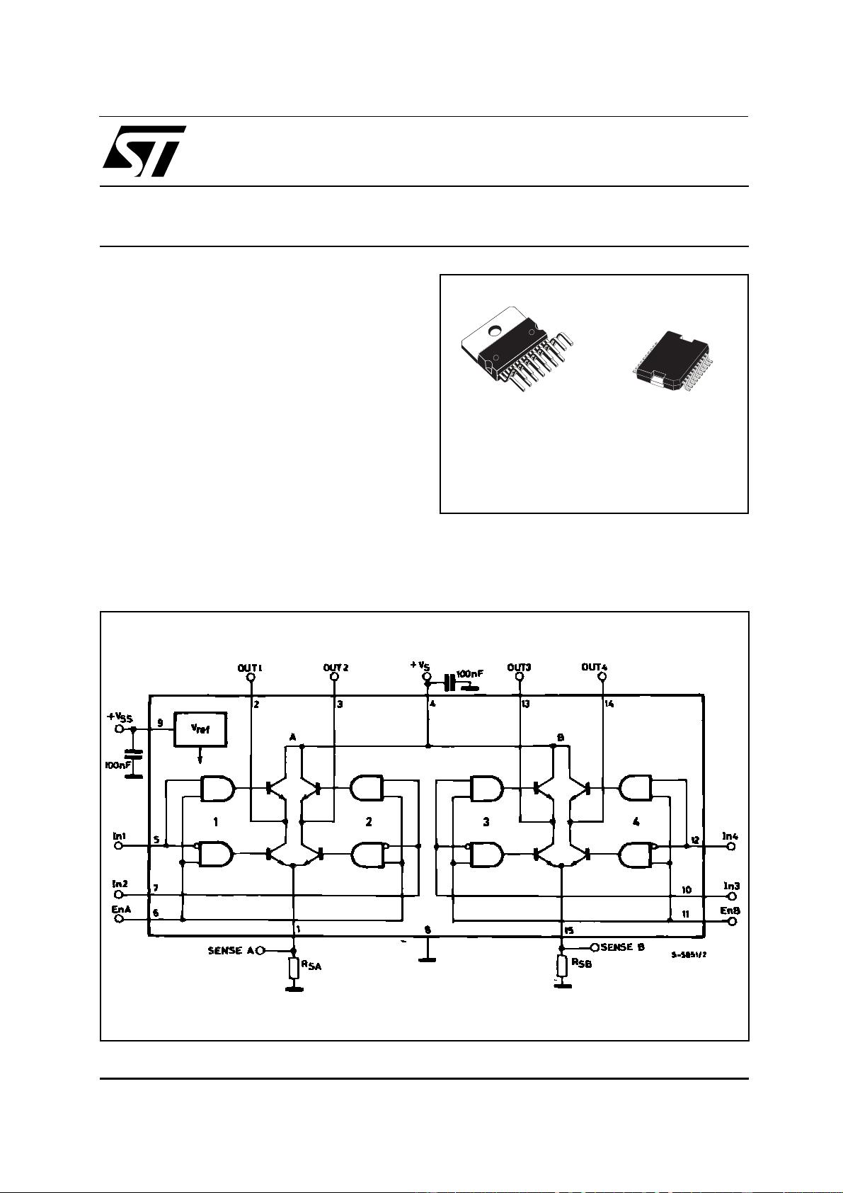
DUAL FULL-BRIDGE DRIVER
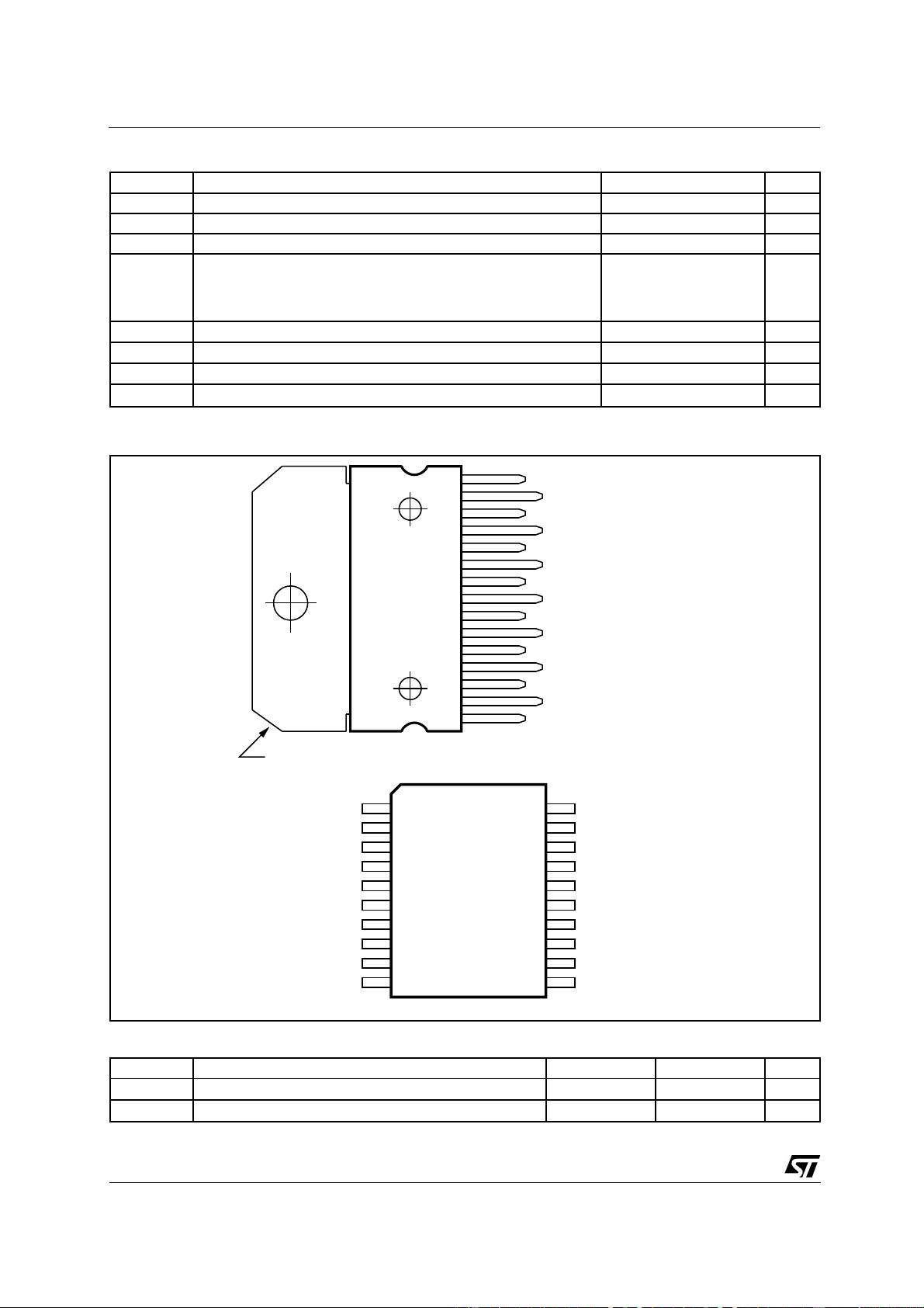
Multiwatt15
ORDERING NUMBERS :
L298N (Multiwatt Vert.)
L298HN (Multiwatt Horiz.)
L298P (PowerSO20)
BLOCK DIAGRAM
.
OPERATING SUPPLY VOLTAGE UP TO 46 V
.
TOTAL DC CURRENT UP TO 4 A
.
LOW SATURATION VOLTAGE
.
OVERTEMPERATURE PROTECTION
.
LOGICAL "0" INPUT VOLTAGE UP TO 1.5 V
(HIGH NOISE IMMUNITY)
DESCRIPTION
The L298 is an integrated monolithic circuit in a 15-
lead Multiwatt and PowerSO20 packages. It is a
high voltage, high current dual full-bridge driver de-
signed to accept standard TTL logic levels and drive
inductive loads such as relays, solenoids, DC and
stepping motors. Two enable inputs are provided to
enable or disable the device independently of the in-
put signals. The emitters of the lower transistors of
each bridge are connected together and the corre-
sponding external terminal can be used for the con-
nection of an external sensing resistor. An additional
supply input is provided so that the logic works at a
lower voltage.
PowerSO20
®
1/13
PIN CONNECTIONS (top view)
GND
Input 2
VSS
N.C.
Out 1
V
S
Out 2
Input 1
Enable A
Sense A
GND 10
8
9
7
6
5
4
3
2
13
14
15
16
17
19
18
20
12
1
11
GND
D95IN239
Input 3
Enable B
Out 3
Input 4
Out 4
N.C.
Sense B
GND
ABSOLUTE MAXIMUM RATINGS
Symbol Parameter Value Unit
V
S
Power Supply 50 V
V
SS
Logic Supply Voltage 7 V
V
I
,V
en
Input and Enable Voltage –0.3 to 7 V
I
O
Peak Output Current (each Channel)
– Non Repetitive (t = 100
µ
s)
–Repetitive (80% on –20% off; t
on
= 10ms)
–DC Operation
3
2.5
2
A
A
A
V
sens
Sensing Voltage –1 to 2.3 V
P
tot
Total Power Dissipation (T
case
= 75
°
C)
25 W
T
op
Junction Operating Temperature –25 to 130
°
C
T
stg
, T
j
Storage and Junction Temperature –40 to 150
°
C
THERMAL DATA
Symbol Parameter PowerSO20 Multiwatt15 Unit
R
th j-case
Thermal Resistance Junction-case Max. – 3
°
C/W
R
th j-amb
Thermal Resistance Junction-ambient Max. 13 (*) 35
°
C/W
(*) Mounted on aluminum substrate
1
2
3
4
5
6
7
9
10
11
8
ENABLE B
INPUT 3
LOGIC SUPPLY VOLTAGE V
SS
GND
INPUT 2
ENABLE A
INPUT 1
SUPPLY VOLTAGE V
S
OUTPUT 2
OUTPUT 1
CURRENT SENSING A
TAB CONNECTED TO PIN 8
13
14
15
12
CURRENT SENSING B
OUTPUT 4
OUTPUT 3
INPUT 4
D95IN240A
Multiwatt15
PowerSO20
L298
2/13
PIN FUNCTIONS (refer to the block diagram)
MW.15 PowerSO Name Function
1;15 2;19 Sense A; Sense B Between this pin and ground is connected the sense resistor to
control the current of the load.
2;3 4;5 Out 1; Out 2 Outputs of the Bridge A; the current that flows through the load
connected between these two pins is monitored at pin 1.
46 V
S
Supply Voltage for the Power Output Stages.
A non-inductive 100nF capacitor must be connected between this
pin and ground.
5;7 7;9 Input 1; Input 2 TTL Compatible Inputs of the Bridge A.
6;11 8;14 Enable A; Enable B TTL Compatible Enable Input: the L state disables the bridge A
(enable A) and/or the bridge B (enable B).
8 1,10,11,20 GND Ground.
9 12 VSS Supply Voltage for the Logic Blocks. A100nF capacitor must be
connected between this pin and ground.
10; 12 13;15 Input 3; Input 4 TTL Compatible Inputs of the Bridge B.
13; 14 16;17 Out 3; Out 4 Outputs of the Bridge B. The current that flows through the load
connected between these two pins is monitored at pin 15.
– 3;18 N.C. Not Connected
ELECTRICAL CHARACTERISTICS (V
S
= 42V; V
SS
= 5V, T
j
= 25°C; unless otherwise specified)
Symbol Parameter Test Conditions Min. Typ. Max. Unit
V
S
Supply Voltage (pin 4) Operative Condition V
IH
+2.5 46 V
V
SS
Logic Supply Voltage (pin 9) 4.5 5 7 V
I
S
Quiescent Supply Current (pin 4) V
en
= H; I
L
= 0 V
i
= L
V
i
= H
13
50
22
70
mA
mA
V
en
= L V
i
= X 4 mA
I
SS
Quiescent Current from V
SS
(pin 9) V
en
= H; I
L
= 0 V
i
= L
V
i
= H
24
7
36
12
mA
mA
V
en
= L V
i
= X 6 mA
V
iL
Input Low Voltage
(pins 5, 7, 10, 12)
–0.3 1.5 V
V
iH
Input High Voltage
(pins 5, 7, 10, 12)
2.3 VSS V
I
iL
Low Voltage Input Current
(pins 5, 7, 10, 12)
V
i
= L –10
µ
A
I
iH
High Voltage Input Current
(pins 5, 7, 10, 12)
Vi = H
≤
V
SS
–0.6V
30 100
µ
A
V
en
= L Enable Low Voltage (pins 6, 11) –0.3 1.5 V
V
en
= H Enable High Voltage (pins 6, 11) 2.3 V
SS
V
I
en
= L Low Voltage Enable Current
(pins 6, 11)
V
en
= L –10
µ
A
I
en
= H High Voltage Enable Current
(pins 6, 11)
V
en
= H
≤
V
SS
–0.6V
30 100
µ
A
V
CEsat (H)
Source Saturation Voltage I
L
= 1A
I
L
= 2A
0.95 1.35
2
1.7
2.7
V
V
V
CEsat (L)
Sink Saturation Voltage I
L
= 1A (5)
I
L
= 2A (5)
0.85 1.2
1.7
1.6
2.3
V
V
V
CEsat
Total Drop I
L
= 1A (5)
I
L
= 2A (5)
1.80 3.2
4.9
V
V
V
sens
Sensing Voltage (pins 1, 15) –1 (1) 2 V
L298
3/13
剩余12页未读,继续阅读
资源评论
Gazier
- 粉丝: 5
- 资源: 50
上传资源 快速赚钱
- 我的内容管理 展开
- 我的资源 快来上传第一个资源
- 我的收益 登录查看自己的收益
- 我的积分 登录查看自己的积分
- 我的C币 登录后查看C币余额
- 我的收藏
- 我的下载
- 下载帮助
最新资源
- J211-T1B-A-VB一款SOT23封装P-Channel场效应MOS管
- J210-VB一款SOT23封装P-Channel场效应MOS管
- J210-T1B-A-VB一款SOT23封装P-Channel场效应MOS管
- Suno V3 AI音乐生成神器,助你秒变音乐大师,suno AI音乐使用教程
- 自适应极化滤波完成P/S波分离
- 0b40adff-950d-44cf-88e6-f4a64292b638.apk
- J209-VB一款SOT23封装P-Channel场效应MOS管
- OLED12864模块(IIC接口)中文说明书.pdf
- 22304010116工管余文贤.bak
- 电路各单元电路的特点与作用
资源上传下载、课程学习等过程中有任何疑问或建议,欢迎提出宝贵意见哦~我们会及时处理!
点击此处反馈
安全验证
文档复制为VIP权益,开通VIP直接复制
信息提交成功