


S3C6400X
USER’S MANUAL
Preliminary_Revision 0.1 (June. 2007)

Important Notice
The information in this publication has been carefully
checked and is believed to be entirely accurate at
the time of publication. Samsung assumes no
responsibility, however, for possible errors or
omissions, or for any consequences resulting from
the use of the information contained herein.
Samsung reserves the right to make changes in its
products or product specifications with the intent to
improve function or design at any time and without
notice and is not required to update this
documentation to reflect such changes.
This publication does not convey to a purchaser of
semiconductor devices described herein any license
under the patent rights of Samsung or others.
Samsung makes no warranty, representation, or
guarantee regarding the suitability of its products for
any particular purpose, nor does Samsung assume
any liability arising out of the application or use of
any product or circuit and specifically disclaims any
and all liability, including without limitation any
consequential or incidental damages.
"Typical" parameters can and do vary in different
applications. All operating parameters, including
"Typicals" must be validated for each customer
application by the customer's technical experts.
Samsung products are not designed, intended, or
authorized for use as components in systems
intended for surgical implant into the body, for other
applications intended to support or sustain life, or for
any other application in which the failure of the
Samsung product could create a situation where
personal injury or death may occur.
Should the Buyer purchase or use a Samsung
product for any such unintended or unauthorized
application, the Buyer shall indemnify and hold
Samsung and its officers, employees, subsidiaries,
affiliates, and distributors harmless against all
claims, costs, damages, expenses, and reasonable
attorney fees arising out of, either directly or
indirectly, any claim of personal injury or death that
may be associated with such unintended or
unauthorized use, even if such claim alleges that
Samsung was negligent regarding the design or
manufacture of said product.
S3C6400X 32-Bit RISC Microcontrollers
User manual, Revision 0.1
Publication Number:
05-S3-C6400X-062007
© 2007 Samsung Electronics
All rights reserved. No part of this publication may be reproduced, stored in a retrieval system, or transmitted in
any form or by any means, electric or mechanical, by photocopying, recording, or otherwise, without the prior
written consent of Samsung Electronics.
Samsung Electronics' microcontroller business has been awarded full ISO-14001
certification (BVQ1 Certificate No. 9330). All semiconductor products are
designed and manufactured in accordance with the highest quality standards
and objectives.
Samsung Electronics Co., Ltd.
San #24 Nongseo-Dong, Giheung- gu
Yongin-City, Gyeonggi-Do, Korea
C.P.O. Box #37, Suwon 446-711
TEL: (82)-(031)-209-1928
FAX: (82)-(031)-209-1909
Home Page: http://www.samsungsemi.com
Printed in the Republic of Korea
S3C6400 RISC MICROPROCESSOR DOCUMENT REVISION HISTORY
1
Preliminary product information describe products that are in development,
for which full characterization data and associated errata are not yet available.
S
p
ecifications and information herein are sub
j
ect to chan
g
e without notice.
DOCUMENT REVISION HISTORY
The following table shows the revision history for this document.
Version Date Revision Descriptions
0.1 June 05, 2007 Initial Release.
PRELIMINARY
S3C6400 RISC MICROPROCESSOR PRODUCT OVERVIEW
1-1
Preliminary product information describe products that are in development,
for which full characterization data and associated errata are not yet available.
Specifications and information herein are subject to change without notice.
1 PRODUCT OVERVIEW
Architectural Overview
The S3C6400 is a 16/32-bit RISC microprocessor, which is designed to provide a cost-effective, low-power
capabilities, high performance Application Processor solution for mobile phones and general applications. To
provide optimized H/W performance for the 2.5G & 3G communication services, the S3C6400 adopts a 64/32-bit
internal bus architecture. The 64/32-bit internal bus architecture is composed of AXI, AHB and APB buses. It also
includes many powerful hardware accelerators for tasks such as motion video processing, audio processing, 2D
graphics, display manipulation and scaling. An integrated Multi Format Codec (MFC) supports encoding and
decoding of MPEG4/H.263/H.264 and decoding of VC1. This H/W Encoder/Decoder supports real-time video
conferencing and TV out for both NTSC and PAL mode.
The S3C6400 has an optimized interface to external memory. This optimized interface to external memory is
capable of sustaining the high memory bandwidths required in high-end communication services. The memory
system has dual external memory ports, DRAM and Flash/ROM/DRAM port. The DRAM port can be configured to
support mobile DDR, DDR, mobile SDRAM and SDRAM. The Flash/ROM/DRAM port supports NOR-Flash,
NAND-Flash, OneNAND, CF, ROM type external memory and mobile DDR, DDR, mobile SDRAM and SDRAM.
To reduce total system cost and enhance overall functionality, the S3C6400 includes many hardware peripherals
such as a Camera Interface, TFT 24-bit true color LCD controller, System Manager (power management & etc.),
4-channel UART, 32-channel DMA, 4-channel Timers, General Purpose I/O Ports, I2S-Bus interface, I2C-BUS
interface, USB Host, USB OTG operating at high speed (480Mbps), SD Host & High Speed Multi-Media Card
Interface and PLLs for clock generation.
For Small Form Factor applications, POP (Package on Package) option with MCP is allowed.
The ARM subsystem is based on the ARM1176JZF-S core. It includes separate 16KB Instruction and 16KB data
caches,
16KB Instruction and 16KB Data TCM. It also includes a full MMU to handle virtual memory management.
The ARM1176JZF-S is a single chip MCU which includes support for JAVA acceleration. The ARM1176JZF-S
includes a dedicated vector floating point coprocessor allowing efficient implementation of various encryption
schemes as well as high quality 3D graphics applications. The S3C6400 adopts the de-facto standard AMBA bus
architecture. These powerful, industry standard features allow the S3C6400 to support many of the industry
standard Operating Systems.
By providing a complete set of common system peripherals, the S3C6400 minimizes overall system costs and
eliminates the need to configure additional components. The S3C6400 is implemented using an advanced 90nm
CMOS process. The low-power, simple, elegant and fully static-design scheme is particularly suitable for cost-
sensitive and power-sensitive applications.
PRELIMINARY
PRODUCT OVERVIEW S3C6400 RISC MICROPROCESSOR
1-2
Preliminary product information describe products that are in development,
for which full characterization data and associated errata are not yet available.
Specifications and information herein are subject to change without notice.
FEATURES
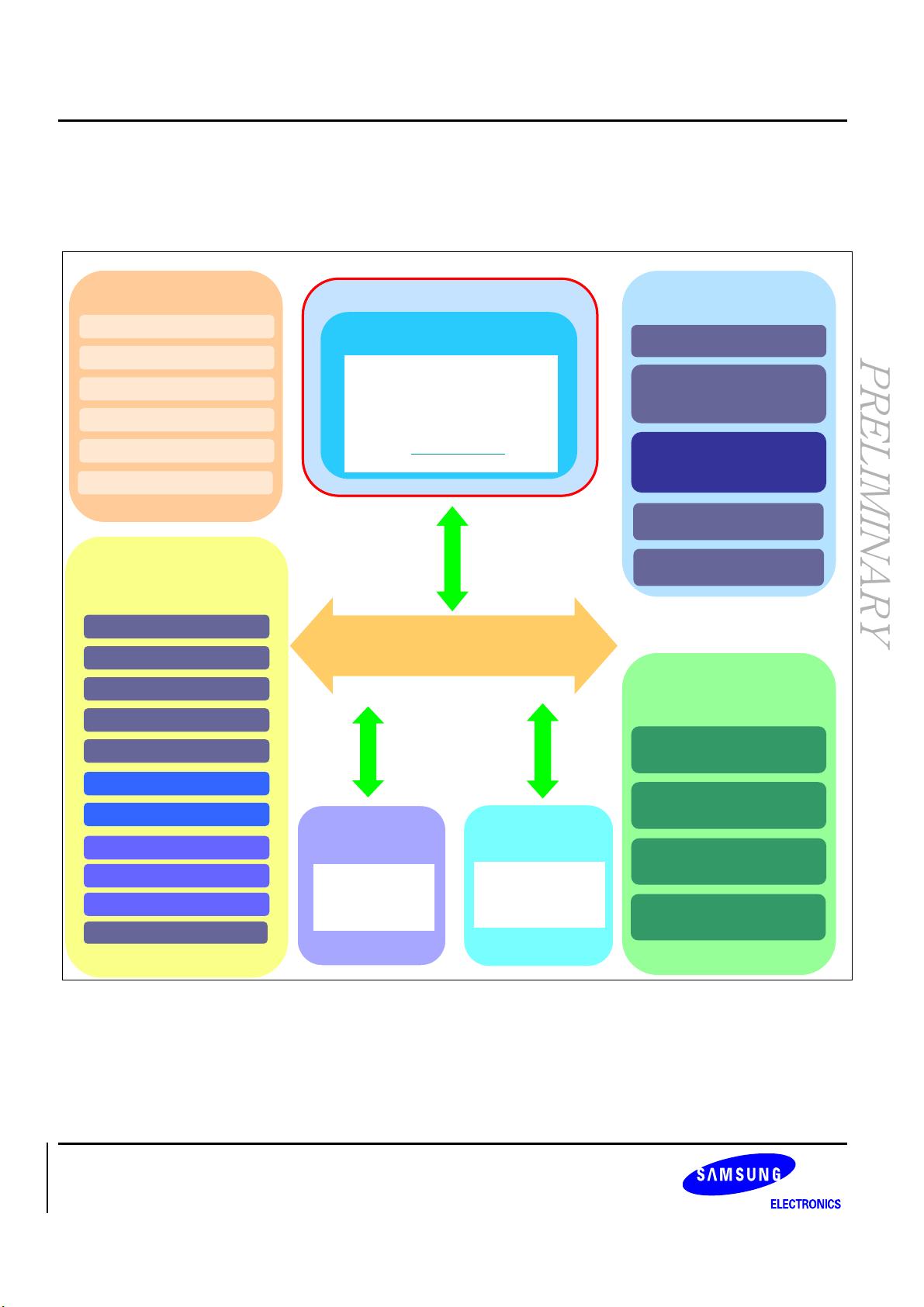
This section summarizes the features of the S3C6400. Figure 1-1 is an overall block diagram of the S3C6400.
UART × 4
Connectivity
USB OTG 2.0
Multimedia
Acceleration
Camera I/F
Multi Format CODEC
(H.264 / MPEG4/ VC1)
X64/32 Multi - Layer AHB/
AXI
AXI Bus
Mobile SDRAM
Mobile DDR SDRAM
Memory Subsystem
Power
Management
TFT LCD
Controller
SRAM/ROM/NOR/
OneNAND
ARM Core
ARM 1176JZF-S
IrDA v1.1
I2S
I2C
GPIO
HS-MMC/SD
Resolution up to
1024x1024
Color-TFT LCD
PLL × 3
RTC
System Peripheral
Timer w/ PWM
Watch Dog Timer
DMA(32 ch)
Keypad (8 x 8)
NTSC, PAL TV out
(with Image
Enhancement)
SPI (Full Duplex)
HSI (Modem I/F)
JPEG
NAND Flash
AC97 / PCM Audio I/F
Normal, Idle
Stop, Sleep
I-Cache 16KB
D-Cache 16KB
I-TCM 16KB
D-TCM 16KB
400/533MHz@TBD
V
USB Host 1.1
2D Graphics
Figure 1-1 S3C6400 block diagram


